Review
. 2017 Mar 24;22(4):520.
doi: 10.3390/molecules22040520.

Morphology Analysis and Optimization: Crucial Factor Determining the Performance of Perovskite Solar Cells

Affiliations
Review

Morphology Analysis and Optimization: Crucial Factor Determining the Performance of Perovskite Solar Cells

Wenjin Zeng et al. Molecules. .

Abstract

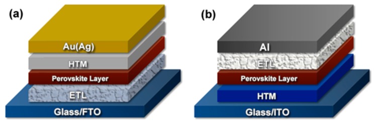
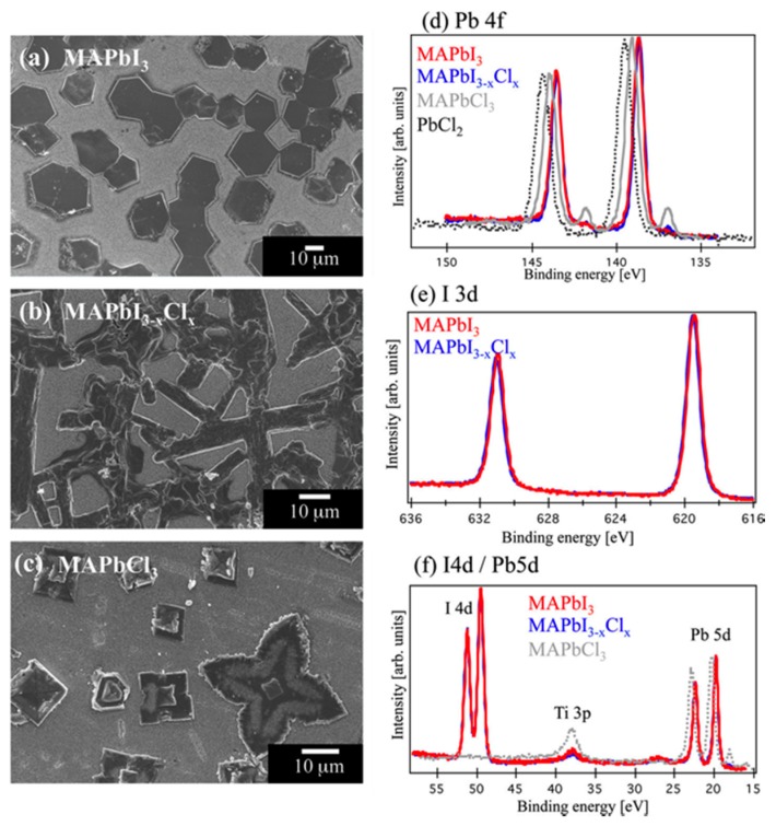
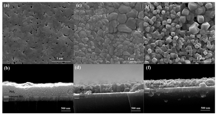
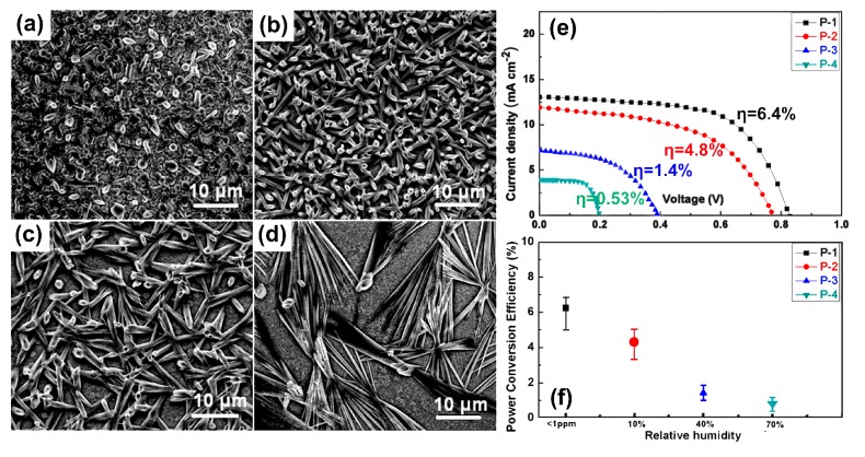
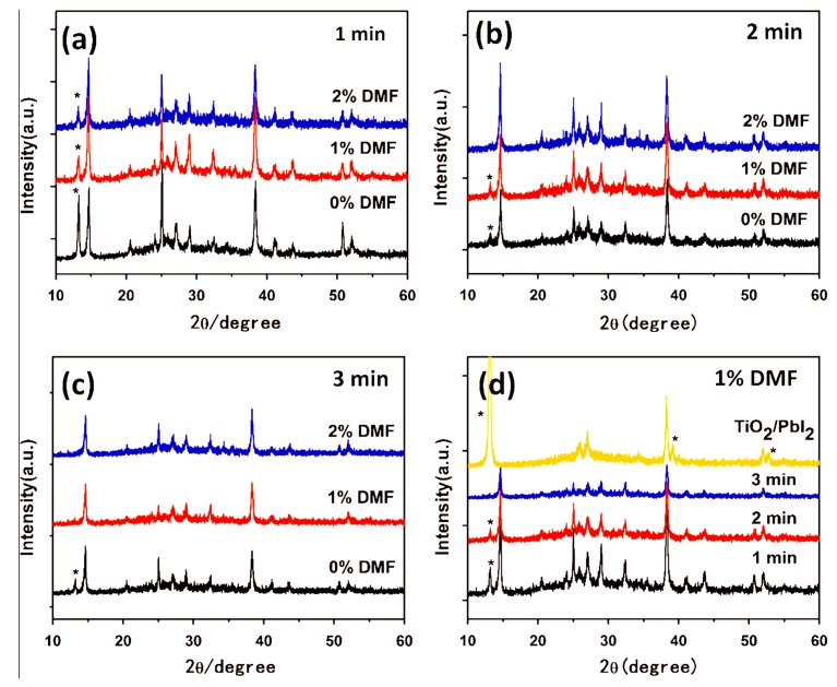
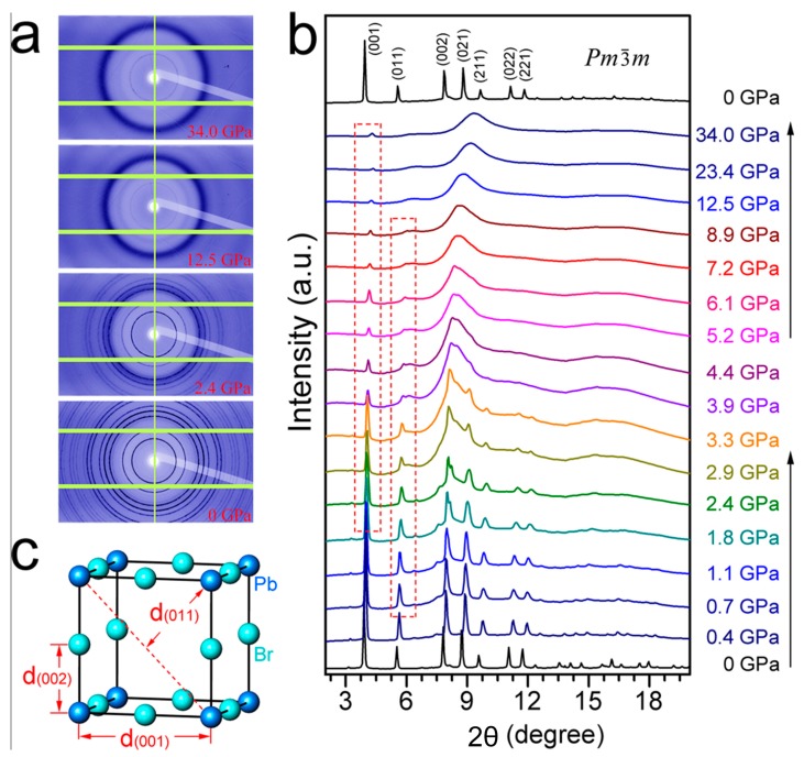
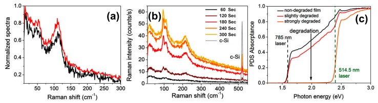
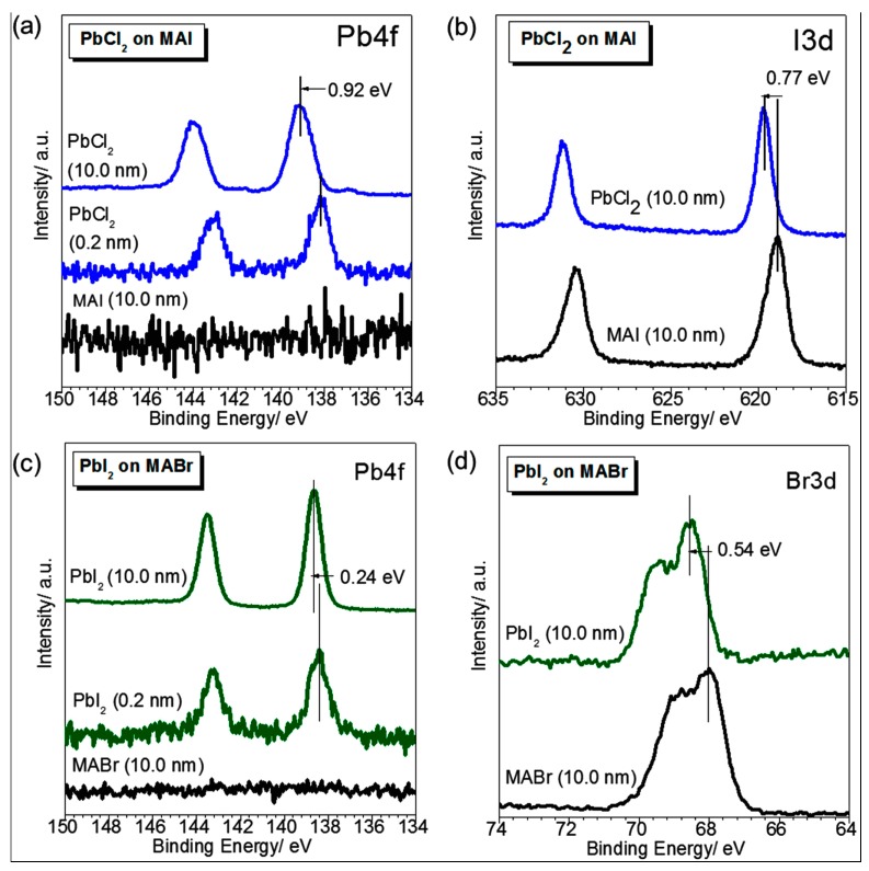
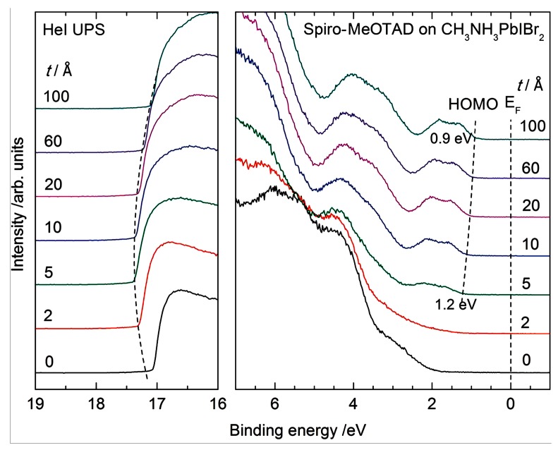
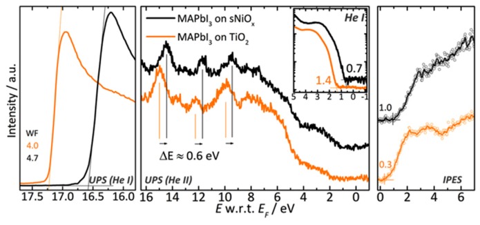
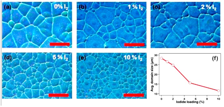
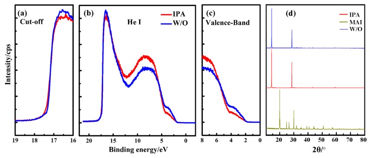
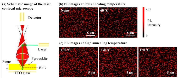
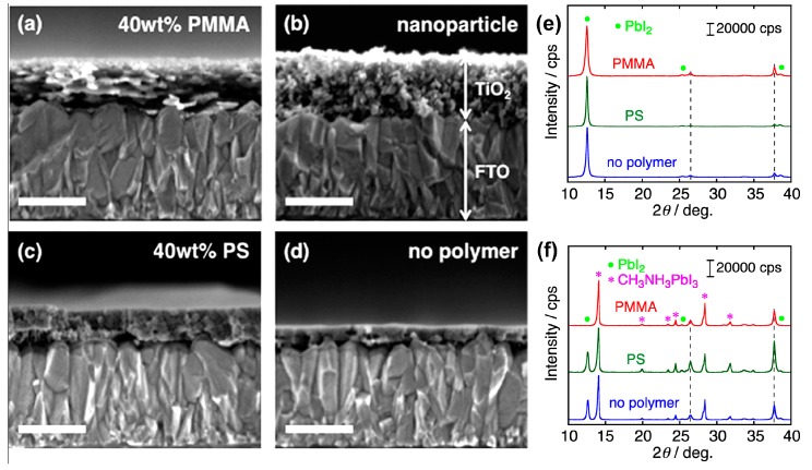
This review presents an overall discussion on the morphology analysis and optimization for perovskite (PVSK) solar cells. Surface morphology and energy alignment have been proven to play a dominant role in determining the device performance. The effect of the key parameters such as solution condition and preparation atmosphere on the crystallization of PVSK, the characterization of surface morphology and interface distribution in the perovskite layer is discussed in detail. Furthermore, the analysis of interface energy level alignment by using X-ray photoelectron spectroscopy and ultraviolet photoelectron spectroscopy is presented to reveals the correlation between morphology and charge generation and collection within the perovskite layer, and its influence on the device performance. The techniques including architecture modification, solvent annealing, etc. were reviewed as an efficient approach to improve the morphology of PVSK. It is expected that further progress will be achieved with more efforts devoted to the insight of the mechanism of surface engineering in the field of PVSK solar cells.

Keywords: CH3NH3PbI3; energy alignment; interface; morphology; perovskite; photovoltaic.


Conflict of interest statement

The authors declare no conflict of interest.

Figures

Figure 1
Figure 1
Structure of PVSK solar cells: (a) conventional device and (b) inverted device.
Figure 2
Figure 2
Top-view SEM images of (a) the MAPbI3 (red frame); (b) MAPbI3−xClx (blue frame); and (c) MAPbCl3 (gray frame) materials deposited on a TiO2/FTO substrate. (Horizontal scale bars = 10 mm.) Also shown are (d) Pb 4f spectra; (e) I 3d spectra; and (f) Pb 5d/I 4d spectra of MAPbI3 (red solid line), MAPbI3−xClx (blue solid line), and MAPbCl3 (light gray line) recorded with an excitation energy of 4000 eV [41]. Copyright © 2015, American Chemical Society, Washington, DC, USA.
Figure 3
Figure 3
Top-view SEM images of (a) PbI2; (c) vapor-crystallized perovskite; and (e) solution-crystallized perovskite; the insets of c and e show magnified images of perovskite crystals. (b,d,f) Corresponding cross-view SEM images of PbI2, vapor crystallized perovskite, and solution-crystallized perovskite [54]. Copyright © 2015, American Chemical Society.
Figure 4
Figure 4
SEM images of perovskite MAPbI3 films deposited on mp-TiO2 layer under different ambient humidities, i.e., (a) <1 ppm (P-1); (b) 10% (P-2); (c) 40% (P-3) and (d) 70% (P-4); (e) J–V curves of the perovskite solar cells prepared under different ambient humidities of MAPbI3; (f) Dependence of the PCEs on RH. Each data point represents the mean from a set of 10 devices [60]. Copyright © 2015, American Chemical Society.
Figure 5
Figure 5
Effect of the ratio of DMF and dipping time on XRD patterns (a) 1 min; (b) 2 min; (c) 3 min; and (d) different dipping time with 1% DMF [76]. Copyright © 2015, Elsevier.
Figure 6
Figure 6
Synchrotron XRD patterns of MAPbBr3 obtained during compression up to 34.0 GPa and decompression: (a) The raw 2D XRD images and (b) integrated 1D XRD profiles. The XRD pattern after decompression can be indexed with the same crystal structure (space group Pm3¯m) from the pristine materials; (c) Illustration of the representative interplanar distances in MAPbBr3 lattice (Only Pb and Br atoms are drawn for clarity) [81]. Copyright © 2015, American Chemical Society.
Figure 7
Figure 7
(a) Normalized Raman spectra measured at two different positions on a pristine MAPbI3 layer using a very low excitation laser power of 10 μW at 514.5 nm; (b) Five Raman spectra measured consecutively without any additional delay time at the same position of a MAPbI3 layer at the excitation wavelength of 514.5 nm in ambient conditions; (c) PDS absorption spectra of MAPbI3 layers at various degradation states. The green and black lines indicate the excitation laser wavelengths used for these experiments (514.5 and 785 nm, respectively) [86]. Copyright © 2015, American Chemical Society.
Figure 8
Figure 8
High-resolution XPS core level spectra of (a) Pb 4f and (b) I 3d when different thicknesses of PbCl2 are deposited on 10.0 nm of MAI. XPS core level spectra of (c) Pb 4f and (d) Br 3d when different thicknesses of PbI2 are deposited on 10.0 nm of MABr [88]. Copyright © 2015, American Chemical Society.
Figure 9
Figure 9
Thickness (t) dependence of UPS spectra of spiro-MeOTAD on MAPbIBr2. The left panel displays the SECO region and the right panel displays the HOMO region, respectively [94]. Copyright © 2015 WILEY-VCH Verlag GmbH & Co. KGaA, Weinheim, Germany.
Figure 10
Figure 10
UPS and IPES spectra of MAPbI3 on sNiOx (black curve) and MAPbI3 on TiO2 (orange curve). The left panel shows the secondary electron cutoff for work function determination. The middle panel shows the He II valence band spectra. The VBM measured with He I is shown in inset. The right panel shows the IPES spectra for the determination of the CBM [95]. Copyright © 2015 WILEY-VCH Verlag GmbH & Co. KGaA, Weinheim, Germany.
Figure 11
Figure 11
Optical micrographs of hybrid perovskite film (scale bar: 50 μm) from precursor with (a) 0%; (b) 1%; (c) 2%; (d) 5%; and (e) 10% iodine solution (40 mM). (f) Average domain size as a function of iodide loading during fabrication. The average domain size decreases as the iodide loading increases [96]. Copyright © 2015, American Chemical Society.
Figure 12
Figure 12
Ultraviolet photoelectron spectroscopy (UPS) of perovskite film with (red line) and without (blue line) IPA treatment on ITO glass substrates, i.e., (a) The secondary electron cut-off; (b) the full UPS spectrum using He I radiation; (c) the valence-band region; and (d) X-ray diffraction of perovskite film with and without IPA treatment on ITO glass substrates [113]. Copyright © 2015, Elsevier.
Figure 13
Figure 13
(a) Schematic image of the laser confocal microscopy and (b,c) the measured spatial PL images from the perovskite films annealed at low and high temperatures, respectively [117]. Copyright © 2015, American Chemical Society.
Figure 14
Figure 14
Cross-sectional SEM images of (a) TiO2 (40 wt %-PMMA); (b) TiO2 (nanoparticle); (c) TiO2 (40 wt %-PS); and (d) TiO2 (without polymer) on FTO/cTiO2 substrates. Scale bars are 200 nm, and Wide-angle XRD patterns of (e) PbI2 and (f) perovskite MAPbI3 films deposited on FTO/cTiO2/TiO2 (40 wt %-PMMA) (red line), FTO/cTiO2/TiO2 (40 wt %-PS) (green line), and FTO/cTiO2/TiO2 (no-polymers) (blue line). Symbols of green solid circle (•) and pink star (*) represent the XRD diffraction peak position of PbI2 and CH3NH3PbI3 [128]. Copyright © 2015, American Chemical Society.

References

    1. Kojima A., Teshima K., Shirai Y., Miyasaka T. Organometal halide perovskites as visible-light sensitizers for photovoltaic cells. J. Am. Chem. Soc. 2009;131:6050–6051. doi: 10.1021/ja809598r. - DOI - PubMed
    1. Lee M.M., Teuscher J., Miyasaka T., Murakami T.N., Snaith H.J. Efficient hybrid solar cells based on meso-superstructured organometal halide perovskites. Science. 2012;338:643–647. doi: 10.1126/science.1228604. - DOI - PubMed
    1. Burschka J., Pellet N., Moon S., Humphry R., Gao P., Nazeeruddin M.K., Gratzel M. Sequential deposition as a route to high-performance perovskite-sensitized solar cells. Nature. 2013;499:316–319. doi: 10.1038/nature12340. - DOI - PubMed
    1. Liu M., Johnston M.B., Snaith H.J. Efficient planar heterojunction perovskite solar cells by vapour deposition. Nature. 2013;501:395–398. doi: 10.1038/nature12509. - DOI - PubMed
    1. Zhou H., Chen Q., Li G., Luo S., Song T., Duan H., Hong Z., You J., Liu Y., Yang Y. Interface engineering of highly efficient perovskite solar cells. Science. 2014;345:542–546. doi: 10.1126/science.1254050. - DOI - PubMed

LinkOut - more resources