. 2017 Mar 10;3(3):e1602076.
doi: 10.1126/sciadv.1602076. eCollection 2017 Mar.

A highly stretchable, transparent, and conductive polymer

Affiliations

A highly stretchable, transparent, and conductive polymer

Yue Wang et al. Sci Adv. .

Abstract

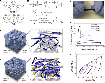
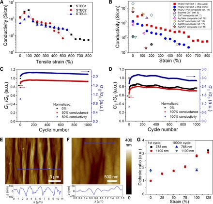
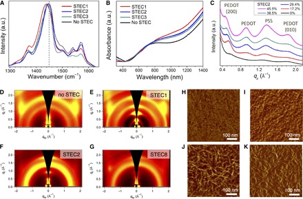
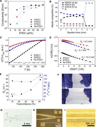
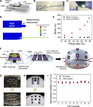
Previous breakthroughs in stretchable electronics stem from strain engineering and nanocomposite approaches. Routes toward intrinsically stretchable molecular materials remain scarce but, if successful, will enable simpler fabrication processes, such as direct printing and coating, mechanically robust devices, and more intimate contact with objects. We report a highly stretchable conducting polymer, realized with a range of enhancers that serve a dual function: (i) they change morphology and (ii) they act as conductivity-enhancing dopants in poly(3,4-ethylenedioxythiophene):poly(styrenesulfonate) (PEDOT:PSS). The polymer films exhibit conductivities comparable to the best reported values for PEDOT:PSS, with over 3100 S/cm under 0% strain and over 4100 S/cm under 100% strain-among the highest for reported stretchable conductors. It is highly durable under cyclic loading, with the conductivity maintained at 3600 S/cm even after 1000 cycles to 100% strain. The conductivity remained above 100 S/cm under 600% strain, with a fracture strain of 800%, which is superior to even the best silver nanowire- or carbon nanotube-based stretchable conductor films. The combination of excellent electrical and mechanical properties allowed it to serve as interconnects for field-effect transistor arrays with a device density that is five times higher than typical lithographically patterned wavy interconnects.

Keywords: Stretchable electronics; conducting polymer; field-effect transistors; ionic dopant; patterning; plasticizer; polymer characterization; rigid-island; soft interface; transparent electrode.


Figures

Fig. 1
Fig. 1. Chemical structures and schematic representation.
(A and B) Chemical structures of PEDOT:PSS (A) and representative STEC enhancers (B) (see complete list in the Supplementary Materials). (C and D) Schematic diagram representing the morphology of a typical PEDOT:PSS film (C) versus that of a stretchable PEDOT film with STEC enhancers (D). (E) Photograph showing a freestanding PEDOT/STEC film being stretched. (F and G) Stress/strain (F) and strain cycling behavior (G) of freestanding PEDOT/STEC films.
Fig. 2
Fig. 2. Electrical and optical properties of stretchable PEDOT under strain.
(A) Conductivity under various strains for PEDOT with different STEC enhancers. Film thicknesses are around 600 to 800 nm. (B) Conductivities under various strain presented in this work compared to representative stretchable conductors reported in literature. PU, polyurethane. (C and D) Cycling stability of PEDOT/STEC1 under 50% strain (C) and 100% strain (D). G, conductance; σ, conductivity; a.u., arbitrary units. (E and F) AFM images of a PEDOT/STEC1 film under different magnifications under 0% strain after it was cycled for 1000 times to 100% strain. The vertical profile across the line on the image is shown below the corresponding image. The deep folds have an amplitude of ~100 nm and a periodicity of ~1.5 μm, whereas those for the wrinkles are ~20 nm and ~0.25 μm, respectively. (G) Dichroic ratio of the PEDOT/STEC1 films under different strains calculated at 785 and 1100 nm for the 1st and the 1000th cycle. There is no change in dichroic ratio from 0 to 100% strain after 1000 cycles, potentially because of the folds formed in the film and a steady concentration of STEC enhancers being reached.
Fig. 3
Fig. 3. Chemical and crystallographic characterization of stretchable PEDOT.
(A) Raman spectra illustrating the Cα=Cβ peak position shift for the different films. The dashed line indicates the peak position for the PEDOT control film without any STEC. (B) UV-vis-NIR spectra showing the doping effect of STEC on PEDOT, as evidenced by increased absorption intensity from bipolaron delocalization at >1000 nm. (C) Near out-of-plane intensity plot of PEDOT:PSS films with various amounts of STEC2 additives extracted from GIWAXS patterns of PEDOT:PSS films with no STEC (D) and 45.5 wt % of STEC1 (E), STEC2 (F), and STEC8 (G) (see also section S3). For the standard PEDOT film without any STEC additives, three peaks were observed along qz: qz = 0.57 Å−1 (d = 11.2 Å), 1.33 Å−1 (d = 4.9 Å), and 1.87 Å−1 (d = 3.4 Å), which can be indexed as PEDOT (200), PSS amorphous scattering, and PEDOT (010), respectively (40, 45). (H to K) AFM phase images of regular PEDOT:PSS (H) compared to PEDOT with high stretchability by incorporating STEC1 (I), STEC2 (J), and STEC3 (K).
Fig. 4
Fig. 4. Electrical properties and patterning of the stretchable PEDOT/STEC (STEC content is 45.5 wt % for all).
(A) Conductivity of the PEDOT films via spin coating followed by various STEC aqueous solution treatments. (B) XPS C60 ion gun sputtering depth profile of a stretchable PEDOT/STEC film. (C) Temperature dependence of the conductivity and (D) Arrhenius fitting for conventional PEDOT compared to those with STEC additives. (E) Sheet resistance of the PEDOT/STEC1 films in relation to their transparency. Transmittance values are extracted at 550 nm. (F) Patterned PEDOT/STEC film on SEBS (top) and the film being stretched (bottom). The line width is 1 mm. (G and H) Photograph (G) and optical microscope image (H) showing micrometer-scale patterns produced by inkjet-printing the PEDOT/STEC. (I) Illustration of the control of feature size, with a line width as small as 40 μm printed on a SEBS substrate.
Fig. 5
Fig. 5. Stretchable PEDOT/STEC as interconnects for LED and FET devices.
(A) Schematic representation of an LED device bridged by PEDOT wires to the power source. (B and C) Photographs illustrating the minimal change in LED brightness as the device is stretched under twisting and poked with a sharp object, respectively. (D) Finite element simulation showing the cross-sectional strain distribution of the rigid-island arrays under 0% (top) and 100% (bottom) strains. (E) Plot summarizing the relationship between array density and strain on PEDOT interconnects when stretching the array to 100% from the simulation results. (F) Schematic diagram of the rigid-island FET array with stretchable PEDOT interconnects. (G and H) Photographs showing the FET array being stretched in all directions on a flat surface and spherical object, respectively. (I) Normalized mobility of individual transistors when the array is stretched to different strains.

References

    1. Wagner S., Bauer S., Materials for stretchable electronics. MRS Bull. 37, 207–213 (2012).
    1. Hammock M. L., Chortos A., Tee B. C.-K., Tok J. B.-H., Bao Z., The evolution of electronic skin (E-skin): A brief history, design considerations, and recent progress. Adv. Mater. 25, 5997–6038 (2013). - PubMed
    1. Jung I., Xiao J., Malyarchuk V., Lu C., Li M., Liu Z., Yoon J., Huang Y., Rogers J. A., Dynamically tunable hemispherical electronic eye camera system with adjustable zoom capability. Proc. Natl. Acad. Sci. U.S.A. 108, 1788–1793 (2011). - PMC - PubMed
    1. Kim D.-H., Ahn J.-H., Mook Choi W., Kim H.-S., Kim T.-H., Song J., Huang Y. Y., Liu Z., Lu C., Rogers J. A., Stretchable and foldable silicon integrated circuits. Science 320, 507–511 (2008). - PubMed
    1. Lipomi D. J., Vosgueritchian M., Tee B. C., Hellstrom S. L., Lee J. A., Fox C. H., Bao Z., Skin-like pressure and strain sensors based on transparent elastic films of carbon nanotubes. Nat. Nanotechnol. 6, 788–792 (2011). - PubMed