Review
. 2013 Aug 27;3(3):524-549.
doi: 10.3390/nano3030524.

Current Trends in Sensors Based on Conducting Polymer Nanomaterials

Affiliations
Review

Current Trends in Sensors Based on Conducting Polymer Nanomaterials

Hyeonseok Yoon. Nanomaterials (Basel). .

Abstract

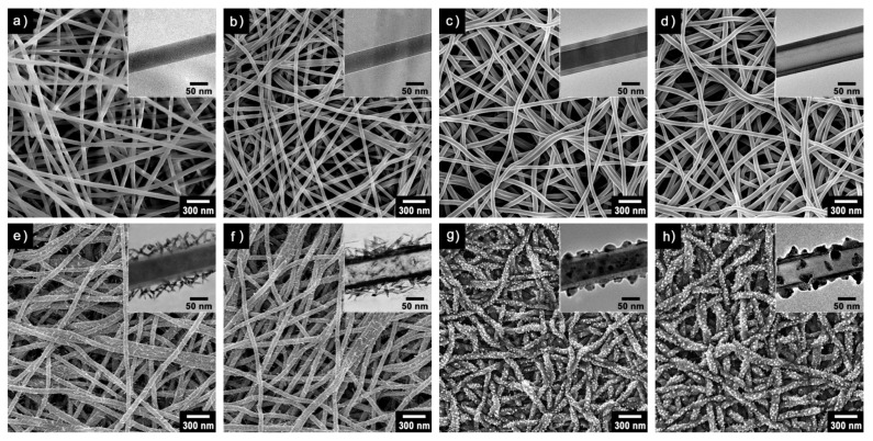
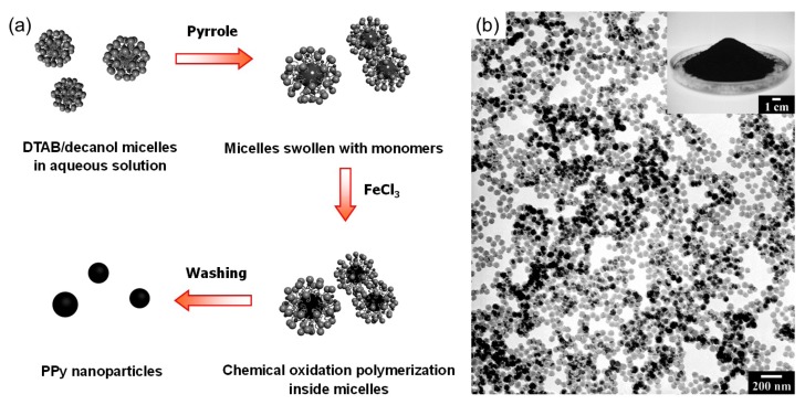
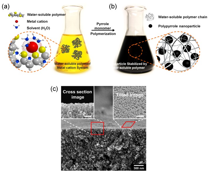
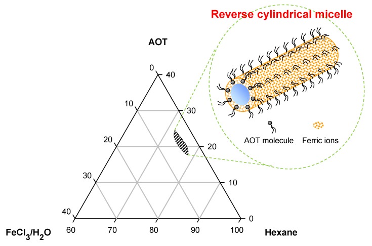
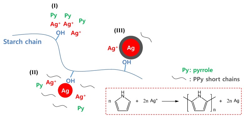
Conducting polymers represent an important class of functional organic materials for next-generation electronic and optical devices. Advances in nanotechnology allow for the fabrication of various conducting polymer nanomaterials through synthesis methods such as solid-phase template synthesis, molecular template synthesis, and template-free synthesis. Nanostructured conducting polymers featuring high surface area, small dimensions, and unique physical properties have been widely used to build various sensor devices. Many remarkable examples have been reported over the past decade. The enhanced sensitivity of conducting polymer nanomaterials toward various chemical/biological species and external stimuli has made them ideal candidates for incorporation into the design of sensors. However, the selectivity and stability still leave room for improvement.

Keywords: biosensors; chemical sensors; conducting polymers; nanomaterials; poly(3,4-ethylenedioxythiophene); polyaniline; polypyrrole.


Conflict of interest statement

The authors declare no conflict of interest.

Figures

Figure 1
Figure 1
Multidimensional poly(3,4-ethylenedioxythiophene) (PEDOT) nanostructures with unique surface substructures. (ah) The poly(methyl methacrylate) (PMMA) nanofibers function as a template and substrate for the growth of PEDOT under different synthetic conditions (temperature and pressure). The morphologies of the resulting nanomaterials were characterized by scanning electron microscopy (SEM) and transmission electron microscopy (TEM) (right top inset images): PMMA nanofibers (a) before and (b) after ferric ion adsorption; PMMA/PEDOT nanofibers with smooth layer surface (c) before and (d) after core etching; PMMA/PEDOT nanofibers with nanorod surface (e) before and (f) after core etching; PMMA/ PEDOT nanofibers with nanonodule surface (g) before and (h) after core etching. With permission from [33]; Copyright 2012, American Chemical Society.
Figure 2
Figure 2
(a) Schematic illustration of the preparation of PPy nanoparticles in a cationic surfactant (DTAB)/co-surfactant (decanol) emulsion system; (b) TEM image of monodisperse PPy nanoparticles prepared through micelle templating (inset: photograph showing a Petri dish containing 12 g of PPy nanoparticles obtained in a single polymerization reaction). With permission from [13]; Copyright 2005, Wiley-VCH Verlag GmbH & Co. KGaA.
Figure 3
Figure 3
Schematic illustration of the formation of PPy nanoparticles in an aqueous dispersion of water-soluble polymer (PVA)/metal cation (ferric ion) complexes, and SEM images of the resulting nanoparticles. (a) Hydroxyl groups of PVA chains coordinate with ferric ions by an ion-dipole interaction in an aqueous medium; (b) The ferric ions act as the oxidizing agent for chemical oxidation of pyrrole monomers. After polymerization, the resulting PPy nanoparticles are stabilized by PVA chains; (c) Tilted and cross-section SEM images of the PPy nanoparticles stacked on a substrate (scale bar: 100 nm). With permission from [34]; Copyright 2010, Wiley-VCH Verlag GmbH & Co. KGaA.
Figure 4
Figure 4
Partial ternary phase diagram for the hexane/AOT/aqueous FeCl3 solution system determined at 15 °C. The molar concentration of the aqueous FeCl3 solution was 16.2 M. The marked area corresponds to the AOT reverse cylindrical micelle phase region. With permission from [22]; Copyright 2005, American Chemical Society.
Figure 5
Figure 5
Schematic illustration of the formation mechanism of Ag-PPy nanoparticles: the reaction process could be divided into three stages (I, II, and III). Right bottom: the scheme describing the chemical reaction between pyrrole and silver cation. With permission from [47]; Copyright 2012, American Chemical Society.
Figure 6
Figure 6
(a) Photograph of a developed gas sensor electrode. SEM images of PPy nanowires deposited on the electrode substrate: (b) 65° tilted view (scale bar = 1 μm) and (c) top view showing PPy nanowires bridging the insulating gap between the gold electrodes (scale bar = 10 μm). With permission from [52]; Copyright 2012, American Chemical Society.
Figure 7
Figure 7
(a) A hybrid nanosensor consisting of a conducting polymer nanojunction (polymer bridged between WE1 and WE2) and a working electrode (WE3) on a Si chip. The chip is covered with a thin layer of ionic liquid (BMIM-PF6) serving as an electrolyte and preconcentration medium. Upon heating TNT particulates (to 60 °C), TNT vapor is generated which is collected by the ionic liquid layer. The analyte is reduced and detected electrochemically on WE3, and the reduction products are detected by the polymer nanojunctions. Inset: Optical micrograph of the sensor chip used and an SEM image of the PEDOT nanojunction; (b) Current (Id) via the PEDOT nanojunction plotted as a function of WE1 potential before and after exposure to TNT; (c) Cyclic voltammograms of a blank BMIM-PF6 solution (black) and 4 ppm TNT in BMIM-PF6 (red). The large reduction current in the latter case is due to the reduction of TNT. Note that an Ag wire quasi-reference electrode and a Pt counter electrode are used. With permission from [55]; Copyright 2010, American Chemical Society.
Figure 8
Figure 8
Sensing performance of chemical nerve agent sensor based on hydroxylated PEDOT nanotubes (HPNTs). (a) Histogram showing the response of HPNTs toward similar organophosphorus compounds at 1 ppb (TCP, MDCP, DMMP, TMP); (b) 3D graphics showing the formation of hydrogen bonds between nerve agent stimulant molecules and HEDOT; (c) Principal components analysis plot using response intensity inputs from four different conducting polymer nanomaterials (two different HPNTs, pristine PEDOT nanotubes, and PPy nanotubes) to the 16 analytes (including DMMP): each analyte concentration was fixed at around 4 ppm. With permission from [59]; Copyright 2012, American Chemical Society.
Figure 9
Figure 9
Schematic structures of the two types of waveguide sensors: (a) conventional waveguide sensor; (b) multilayer integrated waveguide sensor. With permission from [60]; Copyright 2008, American Chemical Society.
Figure 10
Figure 10
Schematic illustration of (a) reaction steps for the fabrication of a sensor platform based on carboxylated PPy nanotubes; and (b) a liquid ion-gated FET sensor; (c) SEM image of carboxylated PPy nanotubes that are deposited on the interdigitated microelectrode substrate. With permission from [62]; Copyright 2008, Wiley-VCH Verlag GmbH & Co. KGaA.
Figure 11
Figure 11
(a) Schematics of maskless electrodeposition of gold along with (b) optical images of before and after selective gold electrodeposition on gold microelectrodes separated by a 3 μm gap connected with a single PPy nanowire; (c) A calibration curve in terms of normalized conductance change of a single PPy nanowire biosensor in spiked human blood plasma suggesting the utility of this sensor for real sample measurements. With permission from [73]; Copyright 2009, American Chemical Society.
Figure 12
Figure 12
(a) The change in resistance of the strain sensor under different external strains; (b) The current response of the strain sensor with cyclical bending and unbending actions of the finger. With permission from [84]; Copyright 2011, Royal Chemical Society.

References

    1. Taur Y., Ning T.H. Fundamental of Modern VLSI Devices. Cambridge University Press; New York, NY, USA: 1998. p. 11.
    1. Dimitrakopoulos C.D., Malenfant P.R.L. Organic thin film transistors for large area electronics. Adv. Mater. 2002;14:99–117. doi: 10.1002/1521-4095(20020116)14:2<99::AID-ADMA99>3.0.CO;2-9. - DOI
    1. Li J., Zhao Y., Tan H.S., Guo Y., Di C.A., Yu G., Liu Y., Lin M., Lim S.H., Zhou Y., et al. A stable solution-processed polymer semiconductor with record high-mobility for printed transistors. Sci. Rep. 2012;2 doi: 10.1038/srep00754. - DOI - PMC - PubMed
    1. Cho S.I., Lee S.B. Fast electrochemistry of conductive polymer nanotubes: Synthesis, mechanism, and application. Acc. Chem. Res. 2008;41:699–707. doi: 10.1021/ar7002094. - DOI - PubMed
    1. Cho S.I., Kwon W.J., Choi S.J., Kim P., Park S.A., Kim J., Son S.J., Xiao R., Kim S.H., Lee S.B. Nanotube-based ultrafast electrochromic display. Adv. Mater. 2005;17:171–175. doi: 10.1002/adma.200400499. - DOI