. 2017 Apr 3:7:45358.
doi: 10.1038/srep45358.

Roles of Oxygen and Hydrogen in Crystal Orientation Transition of Copper Foils for High-Quality Graphene Growth

Affiliations

Roles of Oxygen and Hydrogen in Crystal Orientation Transition of Copper Foils for High-Quality Graphene Growth

Junxiong Hu et al. Sci Rep. .

Abstract

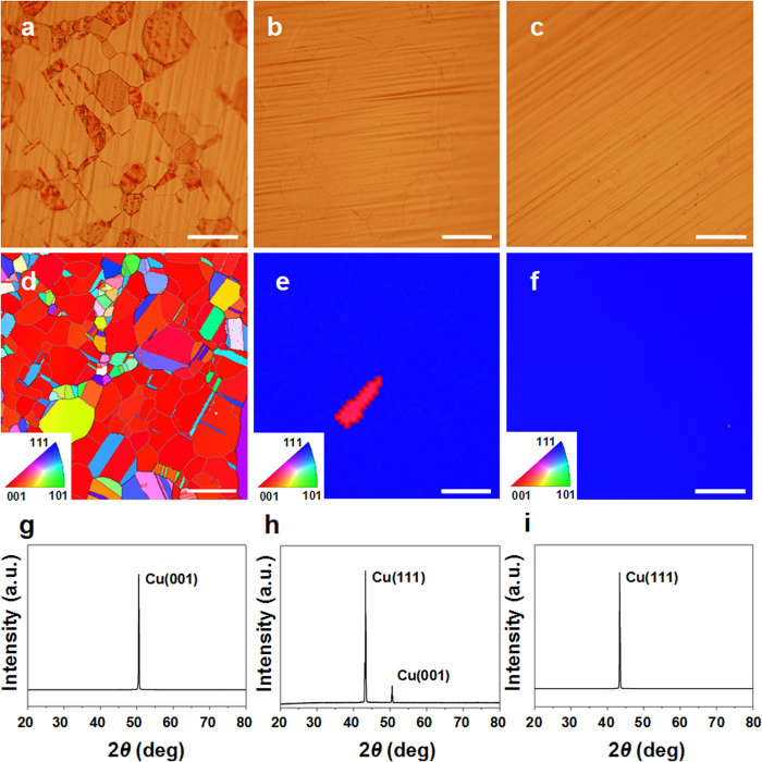
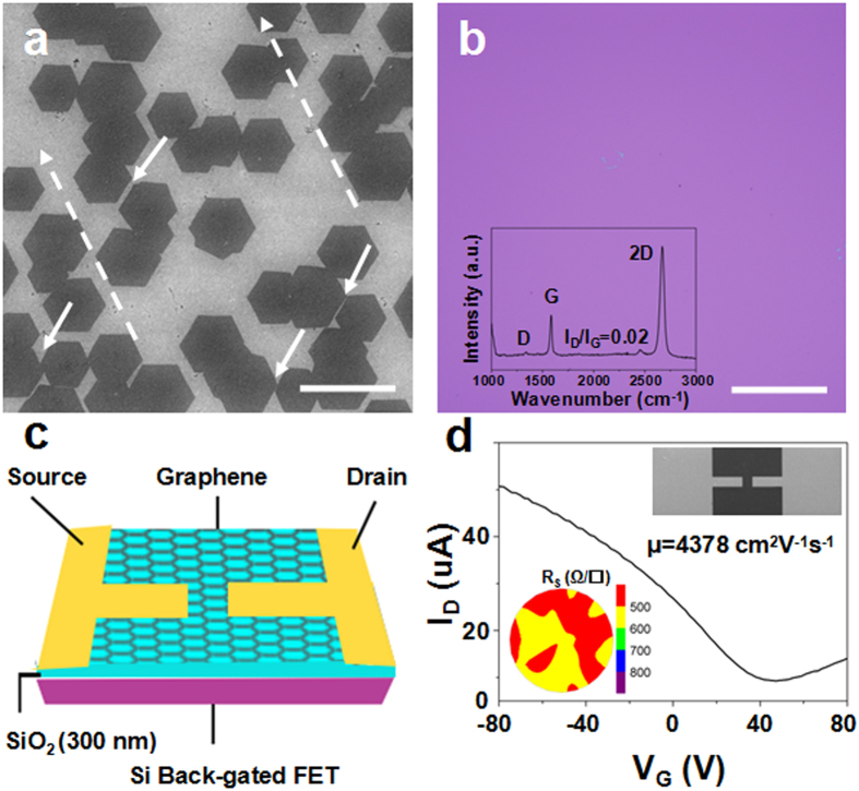
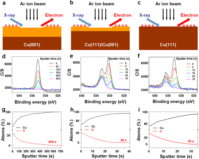
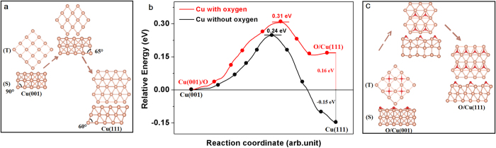
The high-quality graphene film can be grown on single-crystal Cu substrate by seamlessly stitching the aligned graphene domains. The roles of O2 and H2 have been intensively studied in the graphene growth kinetics, including lowering the nucleation sites and tailoring the domain structures. However, how the O2 and H2 influence Cu orientations during recrystallization prior to growing graphene, still remains unclear. Here we report that the oxidation of Cu surface tends to stabilize the Cu(001) orientation while impedes the evolution of Cu(111) single domain during annealing process. The crystal orientation-controlled synthesis of aligned graphene seeds is further realized on the long-range ordered Cu(111) substrate. With decreasing the thickness of oxide layer on Cu surface by introducing H2, the Cu(001) orientation changes into Cu(111) orientation. Meanwhile, the average domain size of Cu foils is increased from 50 μm to larger than 1000 μm. The density functional theory calculations reveal that the oxygen increases the energy barrier for Cu(111) surface and makes O/Cu(001) more stable than O/Cu(111) structure. Our work can be helpful for revealing the roles of O2 and H2 in controlling the formation of Cu single-crystal substrate as well as in growing high-quality graphene films.


Conflict of interest statement

The authors declare no competing financial interests.

Figures

Figure 1
Figure 1. Surface morphology and structure characterizations of Cu foils annealed under 3 schemes.
Scheme 1: heating and annealing under Ar flow. Scheme 2: heating and annealing under H2 and Ar flows, respectively. Scheme 3: heating and annealing under H2 flow. All the samples were heated up to 1040 °C under ambient pressure within 40 min, then annealed at 1040 °C for 30 min. (ac) Optical images of Cu foils annealed under scheme 1–3. Scale bars, 50 μm. (df) EBSD orientation maps of Cu foils annealed under scheme 1–3. The left inset in (df) shows the corresponding inverse pole figure for each map displayed. Grains marked blue are oriented along plane Cu(111) while grains in red are along Cu(001). Scale bars, 200 μm (d,e); 500 μm (f). (gi) XRD profiles of Cu foils annealed under scheme 1–3. The measurements of EBSD and XRD were made from the same area of Cu foils.
Figure 2
Figure 2. Optical and electrical characterizations of graphene grown on singe-domain Cu(111) substrate.
(a) Scanning electron microscope (SEM) image of a partial-coverage aligned graphene seeds on SiO2/Si, where the white dashed lines indicate the orientations of graphene and the arrows point out the coalescence of adjacent islands. Scale bar, 20 μm. (b) Optical image of continuous graphene. The inset shows a representative single-point Raman spectrum. The negligible D band indicates the growth of high-quality graphene film. Scale bar, 20 μm. (c) Schematic of two-point back-gated field-effect-transistor (FET) device. (d) Current − voltage (ID − VG) curve for the continuous graphene grown on Cu(111)-FET measured at room temperature. The right inset shows the SEM image of the device and the left inset shows a representative sheet resistance distribution of graphene film transferred onto SiO2/Si (1.5 mm in diameter).
Figure 3
Figure 3. XPS analysis of the Cu foils annealed under 3 schemes.
(ac) Schematic structures for the XPS depth-profiling of three different thicknesses of copper oxides on corresponding substrate orientations. The orange layer refers to the copper oxides formed during annealing while the top red layer indicates the adsorption of oxygen from air. The thickness is not to scale. (df) Evolution of the O1s peaks as a function of sputter time. The Cu2O peak is at 530.05 eV while the peak of 532.80 eV is attributed to H2O. (gi) Relative atomic contents of O and Cu as a function of sputter time. Using SiO2 as a reference, the corresponding thicknesses of oxidation layers for scheme 1–3 are measured to be 60 nm, 3.6 nm and 3 nm, respectively.
Figure 4
Figure 4. DFT calculations of the effect of oxygen on the orientation transition from Cu(001) to Cu(111).
The side (S) and top (T) views of the Cu surface without oxygen (a) and the favorable oxygen adsorption on Cu surface (c). Note that the oxygen atoms become far away from Cu(111), indicating the weakly bond to the Cu(111) surface. (b) The energy barrier between Cu(001) and Cu(111) without and with oxygen are 0.24 eV and 0.31 eV, respectively.

Similar articles

Cited by

References

    1. Li X. et al.. Large-area synthesis of high-quality and uniform graphene films on copper foils. Science. 324, 1312–1314 (2009). - PubMed
    1. Bae S. et al.. Roll-to-roll production of 30-inch graphene films for transparent electrodes. Nat. Nanotech. 5, 574–578 (2010). - PubMed
    1. Deng B. et al.. Roll-to-roll encapsulation of metal nanowires between graphene and plastic substrate for high-performance flexible transparent electrodes. Nano Lett. 15, 4206–4213 (2015). - PubMed
    1. Huang P. et al.. Grains and grain boundaries in single-layer graphene atomic patchwork quilts. Nature. 469, 389–392 (2011). - PubMed
    1. Kim K. et al.. Grain boundary mapping in polycrystalline graphene. ACS Nano. 5, 2142–2146 (2011). - PubMed

Publication types