. 2017 Apr 18;114(16):4082-4086.
doi: 10.1073/pnas.1620176114. Epub 2017 Apr 3.

Unveiling the carrier transport mechanism in epitaxial graphene for forming wafer-scale, single-domain graphene

Affiliations

Unveiling the carrier transport mechanism in epitaxial graphene for forming wafer-scale, single-domain graphene

Sang-Hoon Bae et al. Proc Natl Acad Sci U S A. .

Abstract

Graphene epitaxy on the Si face of a SiC wafer offers monolayer graphene with unique crystal orientation at the wafer-scale. However, due to carrier scattering near vicinal steps and excess bilayer stripes, the size of electrically uniform domains is limited to the width of the terraces extending up to a few microns. Nevertheless, the origin of carrier scattering at the SiC vicinal steps has not been clarified so far. A layer-resolved graphene transfer (LRGT) technique enables exfoliation of the epitaxial graphene formed on SiC wafers and transfer to flat Si wafers, which prepares crystallographically single-crystalline monolayer graphene. Because the LRGT flattens the deformed graphene at the terrace edges and permits an access to the graphene formed at the side wall of vicinal steps, components that affect the mobility of graphene formed near the vicinal steps of SiC could be individually investigated. Here, we reveal that the graphene formed at the side walls of step edges is pristine, and scattering near the steps is mainly attributed by the deformation of graphene at step edges of vicinalized SiC while partially from stripes of bilayer graphene. This study suggests that the two-step LRGT can prepare electrically single-domain graphene at the wafer-scale by removing the major possible sources of electrical degradation.

Keywords: carrier transport; epitaxial graphene; single crystal; single domain.


Conflict of interest statement

The authors declare no conflict of interest.

Figures

Fig. 1.
Fig. 1.
Optical properties and topography of single-oriented graphene. (A) Four-inch wafer-scale single-oriented graphene on 8-inch oxidized Si wafers via LRGT. (B) Schematic graphene structures before and after LRGT. (C) Map of the 2D/G peak ratio from Raman spectra (green color, monolayer graphene; blue color, bilayer graphene). (D) Tapping mode AFM images from graphene on Si-face SiC wafer and profile information. (E) Tapping mode AFM images from graphene transferred on SiO/Si wafer via LRGT and profile information.
Fig. S1.
Fig. S1.
Raman spectrum of graphene grown on SiC wafer. Raman spectrum was taken with 514-nm wavelength to confirm the quality of graphene. Low D peak intensity and strong G and 2D peak intensity indicate that the quality of graphene is suitable enough to be analyzed.
Fig. 2.
Fig. 2.
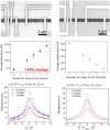
Influence of bilayer stripes. (A) SEM images on graphene FET channels containing one bilayer stripe in a 10-μm-long channel and (B) four bilayer stripes in a 10-μm-long channel. (C) Monotonic increase in average resistance as a function of number of stripes in the channel. The resistance increment by a single bilayer stripe is 1,470 Ω. (D) Average electron FE mobilities of a graphene channel according to the number of stripes in FET channel. (E) Experimentally measured RCH–VG characteristics and (F) simulated RCH–VG characteristics of graphene channel vs. number of stripes.
Fig. S2.
Fig. S2.
Schematic illustration for the graphene transfer and the device fabrication. First, graphene is grown on SiC wafers through graphitization process. After Ni deposition, graphene can be transferred on SiO2/Si substrates. After defining channel areas using e-beam lithography, contact electrodes are prepared through evaporators.
Fig. S3.
Fig. S3.
Scheme for modeling to numerically calculate resistance in bilayer stripes. Scheme shows one example to describe how the channel looks for calculation. The channel consists of four monolayer parts and three bilayer strip parts.
Fig. S4.
Fig. S4.
Contact resistance measurement. The contact resistance measurement through TLM structures with different channel lengths including 0.5, 1, 2, 5, and 10 μm.
Fig. 3.
Fig. 3.
Graphene grown at side-wall surfaces of SiC vicinal steps. (A) SEM images of graphene after LRGT on SiO/Si wafer. FET was fabricated on three different regions: A region, between the bilayer stripes; B region, on the graphene where the stipe was removed during the process; and C region, on the bilayer stripe. (B) FET output characteristics from three different sites at A region, B region, and C region. From the result, we can conclude the device performances from A region and B region are similar, whereas the device performance from C regions shows degradation of mobility. (C and D) Atomic-resolution STM images of single-crystalline graphene from monolayer graphene and bilayer graphene.
Fig. 4.
Fig. 4.
Device performances of monolayer, single-oriented graphene. (A) Raman mapping result of the 2D/G peak ratio on the graphene. Because the bilayer stripes were removed by LRGT, the mapping color is almost uniform. (B) The electron FE mobility distribution comparison between device based on graphene before and after LRGT. (C) Microspot electron diffraction from low-energy electron microscope (LEEM). Identical diffraction patterns across the sample were observed. (D) Channel resistance as a function of gate voltage from single-crystalline graphene. Maximum electron mobility of 7,496 cm2/V⋅s was obtained.
Fig. S5.
Fig. S5.
Transconductance gm as a function of gate voltage Vg for the device with 2 μm of channel width and 1 μm of channel length at VD = 0.01 V.
Fig. S6.
Fig. S6.
Mobility comparison of graphene transistors on SiO2/Si substrate at room temperature (RT). Comparing the mobility results from several studies dealing with graphene grown on Si-face SiC wafers. Maximum mobility of our work is 7,496 cm2/V⋅s, which is the highest value ever reported from graphene grown on Si faces on SiC wafer.
Fig. S7.
Fig. S7.
Topography and corresponding device results before the optimization of the process. (A) AFM was used to see the surface residue on the graphene. (B) Corresponding performance of FETs (2-μm width and 2-μm length).
Fig. S8.
Fig. S8.
Topography and corresponding device results after the optimization of the process. (A) Topographical imaging. AFM image of graphene on the SiO2/Si substrate. There are small nickel residues on the surface. However, we observe no wrinkle on the graphene. (B) Corresponding performance of FETs (2-μm width and 2-μm length).

References

    1. Novoselov KS, et al. Electric field effect in atomically thin carbon films. Science. 2004;306:666–669. - PubMed
    1. Lee C, Wei X, Kysar JW, Hone J. Measurement of the elastic properties and intrinsic strength of monolayer graphene. Science. 2008;321:385–388. - PubMed
    1. Seol JH, et al. Two-dimensional phonon transport in supported graphene. Science. 2010;328(5975):213–216. - PubMed
    1. Zhang Y, Tan Y-W, Stormer HL, Kim P. Experimental observation of the quantum Hall effect and Berry’s phase in graphene. Nature. 2005;438:201–204. - PubMed
    1. Novoselov KS, et al. Two-dimensional gas of massless Dirac fermions in graphene. Nature. 2005;438:197–200. - PubMed