. 2017 Mar 1:8:530-538.
doi: 10.3762/bjnano.8.57. eCollection 2017.

Copper atomic-scale transistors

Affiliations

Copper atomic-scale transistors

Fangqing Xie et al. Beilstein J Nanotechnol. .

Abstract

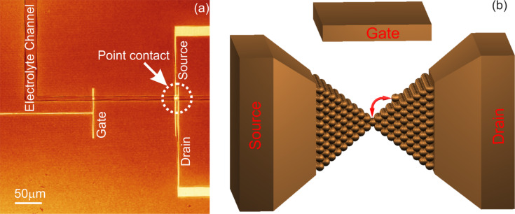
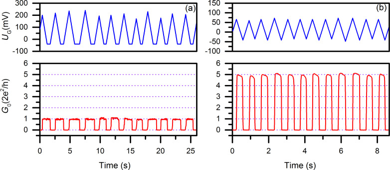
We investigated copper as a working material for metallic atomic-scale transistors and confirmed that copper atomic-scale transistors can be fabricated and operated electrochemically in a copper electrolyte (CuSO4 + H2SO4) in bi-distilled water under ambient conditions with three microelectrodes (source, drain and gate). The electrochemical switching-on potential of the atomic-scale transistor is below 350 mV, and the switching-off potential is between 0 and -170 mV. The switching-on current is above 1 μA, which is compatible with semiconductor transistor devices. Both sign and amplitude of the voltage applied across the source and drain electrodes (Ubias) influence the switching rate of the transistor and the copper deposition on the electrodes, and correspondingly shift the electrochemical operation potential. The copper atomic-scale transistors can be switched using a function generator without a computer-controlled feedback switching mechanism. The copper atomic-scale transistors, with only one or two atoms at the narrowest constriction, were realized to switch between 0 and 1G0 (G0 = 2e2/h; with e being the electron charge, and h being Planck's constant) or 2G0 by the function generator. The switching rate can reach up to 10 Hz. The copper atomic-scale transistor demonstrates volatile/non-volatile dual functionalities. Such an optimal merging of the logic with memory may open a perspective for processor-in-memory and logic-in-memory architectures, using copper as an alternative working material besides silver for fully metallic atomic-scale transistors.

Keywords: electrochemistry; encapsulation; metallic atomic-scale transistor; nanotechnology; photolithography.


Figures

Figure 1
Figure 1
Copper atomic-scale transistor. (a) Confocal optical microscopy image of the microelectrodes, electrolyte channel and the copper point contact (indicated with a dotted circle), which was deposited between the source and the drain. (b) Schematic diagram of an atomic-scale transistor.
Figure 2
Figure 2
The performance of copper atomic-scale transistors. (a) 0–1G0 quantum conductance switching at 0.5 Hz. (b) 0–5G0 quantum conductance switching at 1.5 Hz.
Figure 3
Figure 3
Controlled bistable quantum conductance switching of copper atomic-scale transistors. (a) 0–10G0 switching at 0.57 Hz, UG: −40 mV/210 mV (off/on). (b) 0–11G0 switching at 0.73 Hz, UG: −60 mV/120 mV. (c) 0–12G0 switching at 0.89 Hz, UG: −80 mV/140 mV. (d) 0–13G0 switching at 0.33 Hz, UG: −80 mV/240 mV.
Figure 4
Figure 4
Observation of fabrication and operation of the copper atomic-scale transistor. Confocal microscopy images taken before electrochemical copper deposition, after deposition, and during transistor operation are shown (from left to right).
Figure 5
Figure 5
The operation of a copper atomic-scale transistor driven by a function generator. (a) Schematic diagram of the function-generator-driven copper atomic-scale transistor connected to a current-to-voltage converter circuit. (b) Rectangular wave signal from the function generator (blue) switched between 0 and 300 mV with frequencies from 0.5 Hz to 4 Hz. The output Uout (red), following the signal from the function generator, is driven between 0 and −10.6 V. (c) Zoom-in on the switching sequence from 95 to 100 s.
Figure 6
Figure 6
Demonstration of bistable quantum conductance switching of the copper atomic-scale transistor driven with a function generator. The bistable quantum conductance switching (red) between 0–1G0 (a) and 0–2G0 (b) follow the controlling rectangular wave (blue) at 4 Hz between −105 mV (off) and 275 mV (on) given by the function generator.
Figure 7
Figure 7
Influence of the copper electrolyte additives on the morphology of deposited copper film. (a) Confocal optical microscopy image of the copper atomic-scale transistor taken in situ. (b) The switching performance of the transistor implemented with a rectangular wave signal from a function generator applied to the gate at 10 Hz is plotted in the upper graph (blue). The output signal Uout is in the lower graph (red). The sampling rate of the recording software is 50 samples/s. The solid circles are the measured data and the lines are guides to the eye.

References

    1. Hasegawa T, Terabe K, Tsuruoka T, Aono M. Adv Mater. 2012;24:252–267. doi: 10.1002/adma.201102597. - DOI - PubMed
    1. Lencer D, Salinga M, Wuttig M. Adv Mater. 2011;23:2030–2058. doi: 10.1002/adma.201004255. - DOI - PubMed
    1. Li Y, Long S, Liu Y, Hu C, Teng J, Liu Q, Lv H, Suñé J, Liu M. Nanoscale Res Lett. 2015;10:420. doi: 10.1186/s11671-015-1118-6. - DOI - PMC - PubMed
    1. Waser R, Dittmann R, Staikov G, Szot K. Adv Mater. 2009;21:2632–2663. doi: 10.1002/adma.200900375. - DOI - PubMed
    1. Yang J J, Strukov D B, Stewart D R. Nat Nanotechnol. 2013;8:13–24. doi: 10.1038/nnano.2012.240. - DOI - PubMed