. 2017 Apr 10:7:46314.
doi: 10.1038/srep46314.

Demonstration of nanoimprinted hyperlens array for high-throughput sub-diffraction imaging

Affiliations

Demonstration of nanoimprinted hyperlens array for high-throughput sub-diffraction imaging

Minseop Byun et al. Sci Rep. .

Erratum in

Abstract

Overcoming the resolution limit of conventional optics is regarded as the most important issue in optical imaging science and technology. Although hyperlenses, super-resolution imaging devices based on highly anisotropic dispersion relations that allow the access of high-wavevector components, have recently achieved far-field sub-diffraction imaging in real-time, the previously demonstrated devices have suffered from the extreme difficulties of both the fabrication process and the non-artificial objects placement. This results in restrictions on the practical applications of the hyperlens devices. While implementing large-scale hyperlens arrays in conventional microscopy is desirable to solve such issues, it has not been feasible to fabricate such large-scale hyperlens array with the previously used nanofabrication methods. Here, we suggest a scalable and reliable fabrication process of a large-scale hyperlens device based on direct pattern transfer techniques. We fabricate a 5 cm × 5 cm size hyperlenses array and experimentally demonstrate that it can resolve sub-diffraction features down to 160 nm under 410 nm wavelength visible light. The array-based hyperlens device will provide a simple solution for much more practical far-field and real-time super-resolution imaging which can be widely used in optics, biology, medical science, nanotechnology and other closely related interdisciplinary fields.


Conflict of interest statement

The authors declare no competing financial interests.

Figures
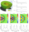
Figure 1
Figure 1. Basic hyperlens structure and simulation results.
(a) Multilayered spherical hyperlens structure. Metal and dielectric thin films are deposited on a spherical shape of substrate. High-frequency information can propagate along the radial direction without decaying and be captured in the far-field. (b) Normalized isofrequency contours of three combinations of materials; Al2O3, TiO2 and GaAs as dielectrics with silver as metal. All combinations satisfy considerably flat hyperbolic dispersion. (ce) The normalized magnetic field distribution is shown in 2D simulations. Sub-wavelength waves propagate along the radial direction further to the far-field and are magnified while passing through the hyperlens in each case: (c) Ag/Al2O3, (d) Ag/TiO2 and (e) Ag/GaAs. The normalized power flux density in the cross-section of the hyperlens is shown for (f) Ag/Al2O3, (g) Ag/TiO2 and (h) Ag/GaAs.
Figure 2
Figure 2. Fabrication procedure of the master stamp for hyperlens.
Figure 3
Figure 3. SEM images of the detailed step-by-step master mold fabrication process.
(a,b) SEM images of the top and cross-section views, respectively, after the lift-off process for a hexagonal array of hole patterns with the dimensions of 700 nm diameter and 3 μm pitch at the Cr layer. (c,d) SEM images of the top and cross-section views, respectively, after the ICP process for a 750 nm diameter and 3 μm pitch hole patterns at the quartz substrate. (e,f) SEM images of the top and cross-section views after all process is finished. Half-spherical patterns array is well defined.
Figure 4
Figure 4
(a) Fabrication procedure of the replicated hyperlens substrate. SEM images of (b,c,d) top view and (e,f,g) tilted view for the quartz master mold, the PDMS mold, and the replicated substrate, respectively.
Figure 5
Figure 5. AFM analysis of the master stamp and the replicated substrate for hyperlens array.
(ac) 3D AFM images of the fabricated patterns on (a) master stamp and (b,c) replicated substrate. The shape has a depth of 1.7 μm and a diameter of 2.5 μm. (de) AFM graph data of the fabricated patterns on the quartz substrate, master stamp (d) and replicated substrate (e), respectively. (f) XPS depth-profiling data of the HAHS-patterned quartz substrate. The carbon signal only exists near the surface region.
Figure 6
Figure 6. TEM images of the cross-section of a replicated hyperlens.
(a,b) TEM images of both ends of the hyperlens. Both parts have the same shape. (c) Ingredients analysis image of the deposited multilayer. (d) Zoom-in TEM image of (c). The thickness of each layer is 15 nm.
Figure 7
Figure 7. Imaging result with the hyperlens integrated microscope setup.
(a) SEM image of the sub-diffraction scale objects. 100 nm diameter holes are separated with distance of 170 nm and the distances between each hole and a bar are 160 nm and 180 nm, respectively. (b) Optics setup. The hyperlens is illuminated by the selected wavelength of light using bandpass filter and transmitted light is captured by objective lens and CCD camera. (c) Far-field optical image after hyperlens. The small object below diffraction limit is clearly resolved by the hyperlens. (d) Cross-sectional intensity profile showing 476 nm distance corresponding to 2.97x magnification factor.

Similar articles

Cited by

References

    1. Abbe E. Beiträge zur Theorie des Mikroskops und der mikroskopischen Wahrnehmung. Archiv für mikroskopische Anatomie 9, 413–418 (1873).
    1. Hillenbrand R. & Keilmann F. Optical oscillation modes of plasmon particles observed in direct space by phase-contrast near-field microscopy. Appl. Phys. B 73, 239–243 (2001).
    1. Rust M. J., Bates M. & Zhuang X. Sub-diffraction-limit imaging by stochastic optical reconstruction microscopy (STORM). Nat. Methods 3, 793–796 (2006). - PMC - PubMed
    1. Betzig E., Trautman J. K., Harris T. D., Weiner J. S. & Kostelak R. L. Breaking the diffraction barrier: Optical microscopy on a nanometric scale. Science 251, 1468–1470 (1991). - PubMed
    1. Hell S. W. Toward fluorescence nanoscopy. Nat. Biotechnol. 21, 1347–1355 (2003). - PubMed

Publication types

LinkOut - more resources