. 2017 May 16;114(20):5107-5112.
doi: 10.1073/pnas.1701478114. Epub 2017 May 1.

Biocompatible and totally disintegrable semiconducting polymer for ultrathin and ultralightweight transient electronics

Affiliations

Biocompatible and totally disintegrable semiconducting polymer for ultrathin and ultralightweight transient electronics

Ting Lei et al. Proc Natl Acad Sci U S A. .

Abstract

Increasing performance demands and shorter use lifetimes of consumer electronics have resulted in the rapid growth of electronic waste. Currently, consumer electronics are typically made with nondecomposable, nonbiocompatible, and sometimes even toxic materials, leading to serious ecological challenges worldwide. Here, we report an example of totally disintegrable and biocompatible semiconducting polymers for thin-film transistors. The polymer consists of reversible imine bonds and building blocks that can be easily decomposed under mild acidic conditions. In addition, an ultrathin (800-nm) biodegradable cellulose substrate with high chemical and thermal stability is developed. Coupled with iron electrodes, we have successfully fabricated fully disintegrable and biocompatible polymer transistors. Furthermore, disintegrable and biocompatible pseudo-complementary metal-oxide-semiconductor (CMOS) flexible circuits are demonstrated. These flexible circuits are ultrathin (<1 μm) and ultralightweight (∼2 g/m2) with low operating voltage (4 V), yielding potential applications of these disintegrable semiconducting polymers in low-cost, biocompatible, and ultralightweight transient electronics.

Keywords: biodegradable materials; conjugated polymers; flexible electronics; organic electronics; thin-film transistors.


Conflict of interest statement

The authors declare no conflict of interest.

Figures
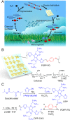
Fig. 1.
Fig. 1.
Schematics of polymer-based transient “green” electronics. (A) Polymer synthesis, fabrication, and decomposition cycle for transient polymer electronics. Solid lines indicate the processes demonstrated in this paper. Dashed lines are the envisioned processes that might be realized in the future. (B) Flexible device using disintegrable polymers as the active material or substrate. Inset shows the fabrication of the cellulose substrate using a reversible functionalization chemistry. (C) Synthesis of the disintegrable PDPP-PD using imine chemistry.
Fig. 2.
Fig. 2.
Degradability and biocompatibility of PDPP-PD. (A) Absorption spectrum changes in PDPP-PD’s decomposition process. (Inset) Photos of polymer solution color changes after decomposition for 10 d and for 40 d. (B) Absorption spectrum changes for a polymer film before and after decomposition in a pH 4.6 buffer solution. (Inset) Photos of the film before and after decomposition. (C) Fluorescent images of live HL-1 cardiomyocytes stained with calcein-AM (green) and EthD-1 (red). (Scale bar: 100 µm.) (D) Viability of HL-1 cardiomyocytes on 2, 4, and 6 d of in vitro culture (n > 1,000 cells for each data bar).
Fig. 3.
Fig. 3.
Characterization of the ultrathin cellulose film and PDPP-PD polymer transistor. (A) Optical transmittance of an 800-nm-thick cellulose film. (Inset) Photo of a cellulose film floating on water. (B) Film thickness changes of a cellulose film soaked in a 1 mg/mL cellulase buffer solution (cellulase from Trichoderma viride; pH 4.6). The film shows a linear decomposition speed of 3.7 nm/h. (C) AFM height image of a cellulose film. (D) 2D-GIXD image of the polymer film (color scale is linear). (E) Transfer and output characteristics of PDPP-PD fabricated on a 800-nm cellulose substrate (50-nm Al2O3, VDS = –10 V).
Fig. 4.
Fig. 4.
Disintegrable pseudo-CMOS circuits based on PDPP-PD. (A) Device structures of the pseudo-CMOS circuits. (B) After dissolving the dextran layer, the device floated on water. (Scale bar: 5 mm.) (C) Device was picked up by a human hair. (Scale bar: 5 mm.) (D) Device was transferred onto the rough surface of an avocado. (Scale bar: 10 mm.) (E) Device transferred onto a PDMS substrate for electrical measurement. (Scale bar: 5 mm.) (F) Device was transferred onto a human brain model. (Scale bar: 5 mm.) (GL) Optical microscopic images, circuit diagrams, and input–output characteristics for different logic gates. (Scale bar: 500 μm.) G and J, Inverter. H and K, NOR gate. I and L, NAND gate. VDD = +4 V, VSS = –4 V.
Fig. 5.
Fig. 5.
Totally disintegrable electronics using iron as electrodes. (A) Schematic of the materials and device structure used for totally disintegrable electronics. (B) Transfer characteristic using Fe as the gate and source-drain electrodes. VDS = –10 V. (C) Photographs of a device at various stages of disintegration. (Scale bars: 5 mm.)

References

    1. Petti L, et al. Metal oxide semiconductor thin-film transistors for flexible electronics. Appl Phys Rev. 2016;3:021303.
    1. Hwang S-W, et al. 25th anniversary article: Materials for high-performance biodegradable semiconductor devices. Adv Mater. 2014;26:1992–2000. - PubMed
    1. Hwang S-W, et al. A physically transient form of silicon electronics. Science. 2012;337:1640–1644. - PMC - PubMed
    1. Irimia-Vladu M. “Green” electronics: Biodegradable and biocompatible materials and devices for sustainable future. Chem Soc Rev. 2014;43:588–610. - PubMed
    1. Bettinger CJ, Bao Z. Organic thin-film transistors fabricated on resorbable biomaterial substrates. Adv Mater. 2010;22:651–655. - PMC - PubMed

Publication types