

Coulomb engineering of the bandgap and excitons in two-dimensional materials
- PMID: 28469178
- PMCID: PMC5418602
- DOI: 10.1038/ncomms15251
Coulomb engineering of the bandgap and excitons in two-dimensional materials
Abstract
The ability to control the size of the electronic bandgap is an integral part of solid-state technology. Atomically thin two-dimensional crystals offer a new approach for tuning the energies of the electronic states based on the unusual strength of the Coulomb interaction in these materials and its environmental sensitivity. Here, we show that by engineering the surrounding dielectric environment, one can tune the electronic bandgap and the exciton binding energy in monolayers of WS2 and WSe2 by hundreds of meV. We exploit this behaviour to present an in-plane dielectric heterostructure with a spatially dependent bandgap, as an initial step towards the creation of diverse lateral junctions with nanoscale resolution.
Conflict of interest statement
The authors declare no competing financial interests.
Figures
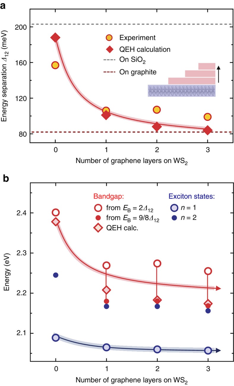
 and the 2D-hydrogen model in a homogeneous dielectric
  . These are compared to the bandgap energies deduced from the calculated exciton binding energies using the QEH model. The solid lines are guides to the eye.
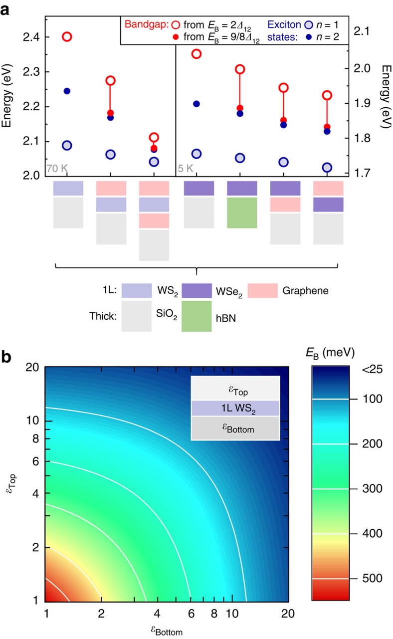
 and the 2D-hydrogen model
  . (b) An overview of predicted changes in the exciton binding energy in 1L WS2, encapsulated between two thick layers of dielectrics. The binding energy EB is calculated by using the electrostatic approach in the effective mass approximation and presented in a 2D false-colour plot as a function of the top and bottom dielectric constants. The changes in the magnitude of EB are roughly equal to the corresponding shifts of the bandgap and can reach 500 meV.
References
-
- Capasso F. Band-gap engineering: from physics and materials to new semiconductor devices. Science 235, 172–176 (1987). - PubMed
-
- Klingshirn C. Semiconductor Optics 3rd edn Springer (2007).
-
- Splendiani A. et al.. Emerging photoluminescence in monolayer MoS2. Nano Lett. 10, 1271–1275 (2010). - PubMed
-
- Mak K. F., Lee C., Hone J., Shan J. & Heinz T. F. Atomically thin MoS2: a new direct-gap semiconductor. Phys. Rev. Lett. 105, 136805 (2010). - PubMed
Publication types
LinkOut - more resources
Full Text Sources
Other Literature Sources
