Review
. 2017 Apr;473(2200):20160889.
doi: 10.1098/rspa.2016.0889. Epub 2017 Apr 12.

Multifunctional scanning ion conductance microscopy

Affiliations
Review

Multifunctional scanning ion conductance microscopy

Ashley Page et al. Proc Math Phys Eng Sci. 2017 Apr.

Abstract

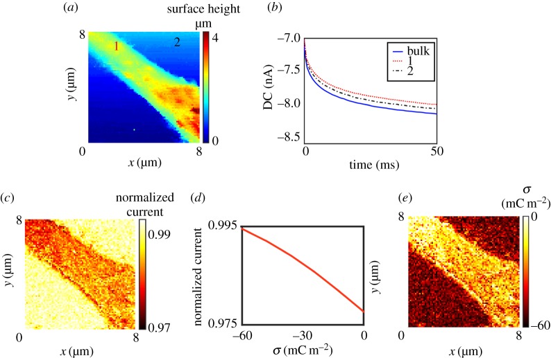
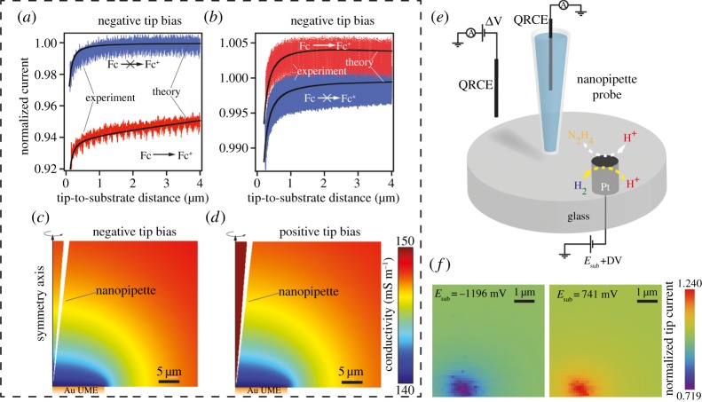
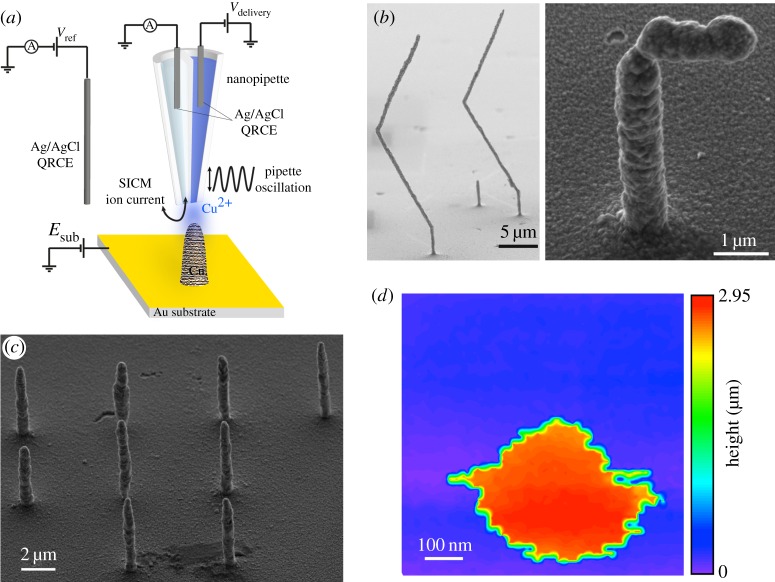
Scanning ion conductance microscopy (SICM) is a nanopipette-based technique that has traditionally been used to image topography or to deliver species to an interface, particularly in a biological setting. This article highlights the recent blossoming of SICM into a technique with a much greater diversity of applications and capability that can be used either standalone, with advanced control (potential-time) functions, or in tandem with other methods. SICM can be used to elucidate functional information about interfaces, such as surface charge density or electrochemical activity (ion fluxes). Using a multi-barrel probe format, SICM-related techniques can be employed to deposit nanoscale three-dimensional structures and further functionality is realized when SICM is combined with scanning electrochemical microscopy (SECM), with simultaneous measurements from a single probe opening up considerable prospects for multifunctional imaging. SICM studies are greatly enhanced by finite-element method modelling for quantitative treatment of issues such as resolution, surface charge and (tip) geometry effects. SICM is particularly applicable to the study of living systems, notably single cells, although applications extend to materials characterization and to new methods of printing and nanofabrication. A more thorough understanding of the electrochemical principles and properties of SICM provides a foundation for significant applications of SICM in electrochemistry and interfacial science.

Keywords: cellular imaging; charge mapping; electrochemical imaging; nanopipette; scanning ion conductance microscopy; single-cell analysis.


Conflict of interest statement

We declare we have no competing interests.

Figures

Figure 1.
Figure 1.
(a) Schematic of the SICM set-up with a nanopipette filled and bathed in electrolyte solution above a substrate of interest. A bias is applied between a QRCE in the nanopipette and one in bulk solution in order to generate an ionic current that can be used as a means of the nanopipette sensing the surface. (b) Simulated resistance approach curve of a nanopipette, with 100 nm diameter, approaching an uncharged surface at 300 mV tip bias in 10 mM KCl. Upon approaching within about one tip diameter of the surface, an increase in the resistance is observed due to the reduced access of ions to the probe opening. (c) Corresponding ionic current as a function of tip–substrate distance from the simulation in (b). (d) Topographical image of three PC12 cells, with surface heights extracted from the point of closest approach at each pixel (hopping mode scan regime).
Figure 2.
Figure 2.
The SICM probe is typically employed in one of two scanning regimes, either with a fixed probe–substrate separation in constant-distance mode (a) with a raster or spiral scan profile (b) or by hopping across the surface (c). Schematic depiction of three SICM feedback types. In the DC approach (d), a decrease in the ionic current is usually used to sense the substrate. In DM-SICM (e), an oscillation is applied to the z-piezoelectric positioner controlling the tip, generating an AC current between the two QRCEs, the magnitude of which is only significant when the nanopipette approaches the substrate. In BM-SICM (f), an oscillation is applied to the bias between the QRCE in the nanopipette and that in bulk solution, generating an AC signal, which is sensitive to the substrate even when zero net bias is applied between the QRCEs. (d–f) Adapted with permission from [12]. Copyright © 2016 American Chemical Society.
Figure 3.
Figure 3.
(a) Typical equivalent circuit diagram to explain the BM-SICM response, where Rbulk, Racc and Rp represent the resistance of the bulk solution, the access resistance and the probe resistance, respectively, while C is the capacitance across the wall of the pipette. (b) Experimental approach curves (tip current response as a function of tip-radius-normalized distance between the tip and surface) of a 75 nm radius (ro) borosilicate glass nanopipette to a glass surface at 0 V net bias in 100 mM KCl solution (10 mV modulation amplitude and 270 Hz frequency), showing the change in AC phase and amplitude with tip–substrate separation. (c) BM-SICM impedance data of the system in (b) with the nanopipette in bulk (black line) and at tip–substrate distances of approximately 150 nm (red line), 100 nm (green line) and 50 nm (blue line). Upon approach to an interface with no net bias, the impedance can be seen to increase.
Figure 4.
Figure 4.
Topographical imaging with BM-SICM showing: (a) a polystyrene film on glass; (b) a PC12 cell and (c) a gold ultramicroelectrode. Note that there is no interpolation of data, and each pixel shown represents a measurement point.
Figure 5.
Figure 5.
Characterization of nanopipette geometry with SEM and TEM showing typical SEM (a) and TEM (b) images of quartz nanopipettes and a TEM image of a borosilicate nanopipette (c). (d) Plot of the inner angle of a typical quartz nanopipette as a function of the height of the nanopipette (measured from the opening). (b–d) Reproduced with permission from [87]. Copyright © 2016 American Chemical Society.
Figure 6.
Figure 6.
(a) Simulated current–voltage curves for a nanopipette in bulk solution with varying surface charge applied to the nanopipette walls. The nanopipette had an opening of radius 90 nm, and the geometry can be gleaned from (b–d) which are two-dimensional concentration profiles for a surface charge of −20 mC m−2 applied to the nanopipette walls with an initial concentration of 10 mM KCl both in the probe and in bulk solution and an applied tip bias with respect to the bulk, VDC, of −0.4 V (b), 0 V (c) and +0.4 V (d). (e–g) One-dimensional profiles of K+ concentration at a fixed height of 4 µm into the pipette, against applied surface charge at −0.4 V (e), 0 V (f) and +0.4 V (g). The key for surface charge in (a) and (e–g) is the same.
Figure 7.
Figure 7.
FEM simulated SICM approach curves at (a) +0.4 V tip bias and (b) −0.4 V tip bias to different charged surfaces (see key), with tip geometry as defined in (e–h). (c) Working surface, at a tip–substrate separation of 10 nm, of tip current normalized to the current with the tip in bulk, as a function of substrate charge and tip bias for a nanopipette wall charge of −20 mC m−2. (d) Working curves of normalized tip current against surface charge for three tip biases. (e–h) Concentration profiles in the region of a nanopipette (axisymmetric cylindrical geometry; r is the radial coordinate starting at the axis of symmetry) near a positively charged substrate, +40 mC m−2 (f,h) and negatively charged substrate, −40 mC m−2 (e,g) with tip biases of −0.4 V (e,f) and +0.4 V (g,h).
Figure 8.
Figure 8.
FEM simulated I–V curves with a 90 nm radius nanopipette in bulk solution in (a) 10 mM KCl, surface charge −5 mC m−2, (b) 100 mM KCl, surface charge −5 mC m−2, (c) 10 mM KCl, surface charge −10 mC m−2 and (d) 100 mM KCl, surface charge −10 mC m−2. Blue lines are simulated results with EOF included, whereas orange lines are the results where EOF is excluded.
Figure 9.
Figure 9.
Nyquist plots representing impedance data for an SICM configuration, with a nanopipette in 10 mM KCl aqueous solution (approx. pH 6.5) with a 10 mV oscillation applied on top of a fixed bias of (a) 0 V, (b) −0.4 V and (c) 0.4 V. The nanopipette was positioned either in bulk solution (blue) or near a glass substrate (orange). Data points corresponding to decades in frequency are denoted by stars and labelled according to the frequency.
Figure 10.
Figure 10.
BM-SICM topography and surface charge mapping of Baker's yeast cells (a–c) and root hair cells (d–f) in 10 mM KCl with the presentation of optical images (a,d), topographical data (b,e) and normalized ionic current data at a bias of 0.4 V (c,f), as a proxy for surface charge. The scan areas are represented on the optical images by a black dashed square.
Figure 11.
Figure 11.
Surface charge mapping of a PC12 cell in physiological conditions, RPMI cell media (approx. 150 mM ionic strength), using pulsed-potential SICM. (a) Topographical map obtained at an approach bias of +20 mV. (b) Example current–time curves extracted in bulk and near the substrate (over the cell and glass support, see (a) for locations) after pulsing the applied bias at the probe QRCE to −400 mV versus bulk. (c) Map of normalized SICM current (current from the surface pulse divided by current during bulk pulse at 50 ms). (d) Simulated working curve at 50 ms to convert (c) to surface charge values (e) at the probe working distance of 30 nm. Adapted with permission from [44]. Copyright © 2016 American Chemical Society.
Figure 12.
Figure 12.
(a,b) Experimental (red and blue traces) and simulated (solid black lines) SICM current–distance curves acquired with a nanopipette (biased at −0.1 and +0.1 V, respectively) positioned over an inert (blue) and Fc+ generating (diffusion-controlled rate) from the oxidation of Fc (Ferrocene methanol) in bulk solution (1.95 mM) at a 12.5 µm radius Au UME (red). Note the difference in scales between (a) and (b). Tuning the tip potential makes the SICM response sensitive (a) or relatively immune (b) to the substrate reaction. (c,d) Simulated conductivity distributions (magnified view) with a nanopipette (biased at ±0.1 V) positioned at 1 µm distance from an Fc+ generating substrate electrode (Au UME). (e) Schematic of the experimental set-up employed for mapping hydrazine oxidation and proton reduction at approximately 600 nm radius Pt UME. (f) Electrochemical images from a 380-snapshot image sequence, constructed from voltammetric data resolved at each image pixel. The nanopipette current has been normalized by the value at the point of the closest approach (at each individual pixel) with the substrate potential held at −0.2 V (no substrate reaction). Adapted with permission from [43]. Copyright © 2016 American Chemical Society.
Figure 13.
Figure 13.
Deposition of Cu nanostructures with a dual-barrel nanopipette. (a) Schematic of the experimental set-up, with one barrel of the theta pipette used for SICM feedback and the other used as a source of Cu2+ ions. (b) Array of nine pillars deposited at a substrate potential of −0.75 V (versus Ag/AgCl QRCE) with an SICM bias of 0.2 V and a bias in the Cu reservoir barrel of 1 V (versus same QRCE). The deposition time was 60 s and the probe was translated away from the surface under positional feedback control during the growth of each feature. (c) Example scanning electron micrographs of Cu nanostructures created by retracting vertically before moving laterally with and without feedback to create zig-zag and gamma structures (left- and right-hand images, respectively). (d) Hopping mode SICM image of a deposited Cu pillar, taken with the same nanopipette probe as used for patterning. Adapted with permission from [39]. Copyright © 2016 American Chemical Society.
Figure 14.
Figure 14.
Potentiometric scanning ion conductance microscopy (P-SICM). (a) Schematic of the P-SICM experimental set-up. A bias is applied between the working electrode (WE) and the counter electrode (CE) while the pipette electrode (PE) measures topography and the potential electrode (UE) records the local potential at the pipette tip to make conductance measurements. All electrode potentials are referenced to a single reference electrode (RE). (b) Local potential variation at nanopores in a polymer membrane at three different transmembrane potentials, measured using P-SICM in imaging mode. Scale bar, 1 µm. (c) Topographical image of the surface of a cell monolayer shows the position of cell bodies and cell junctions. Scale bar, 5 µm. The inset shows the zoom out image of the cell monolayer under study (40 × 40 µm). CB indicates the cell body and CJ the cell junction. (d) Histograms of conductances measured at cell junctions for two cell strains (MDCKII-WT and MDCKII-C2, red and blue, respectively) using P-SICM, showing that claudin-2 regulates epithelial permeability. (b–d) Reproduced with permission from Dr Lane A. Baker from [88]. Copyright © 2014 The Electrochemical Society.

Similar articles

Cited by

References

    1. Hansma PK, Drake B, Marti O, Gould SA, Prater CB. 1989. The scanning ion-conductance microscope. Science 243, 641–643. (doi:10.1126/science.2464851) - DOI - PubMed
    1. Korchev YE, Bashford CL, Milovanovic M, Vodyanoy I, Lab MJ. 1997. Scanning ion conductance microscopy of living cells. Biophys. J. 73, 653–658. (doi:10.1016/S0006-3495(97)78100-1) - DOI - PMC - PubMed
    1. Gorelik J, et al. 2004. The use of scanning ion conductance microscopy to image A6 cells. Mol. Cell. Endocrinol. 217, 101–108. (doi:10.1016/j.mce.2003.10.015) - DOI - PubMed
    1. Chen C-C, Zhou Y, Baker LA. 2012. Scanning ion conductance microscopy. Annu. Rev. Anal. Chem. 5, 207–228. (doi:10.1146/annurev-anchem-062011-143203) - DOI - PubMed
    1. Meyer E, Hug HJ, Bennewitz R. 2013. Scanning probe microscopy: the lab on a tip. Berlin, Germany: Springer Science & Business Media.

LinkOut - more resources