. 2017 May 23;7(1):2282.
doi: 10.1038/s41598-017-02511-8.

A Simple Silver Nanowire Patterning Method Based on Poly(Ethylene Glycol) Photolithography and Its Application for Soft Electronics

Affiliations

A Simple Silver Nanowire Patterning Method Based on Poly(Ethylene Glycol) Photolithography and Its Application for Soft Electronics

Youngsang Ko et al. Sci Rep. .

Abstract

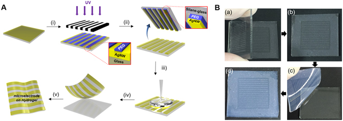
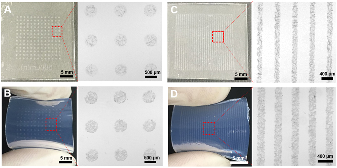
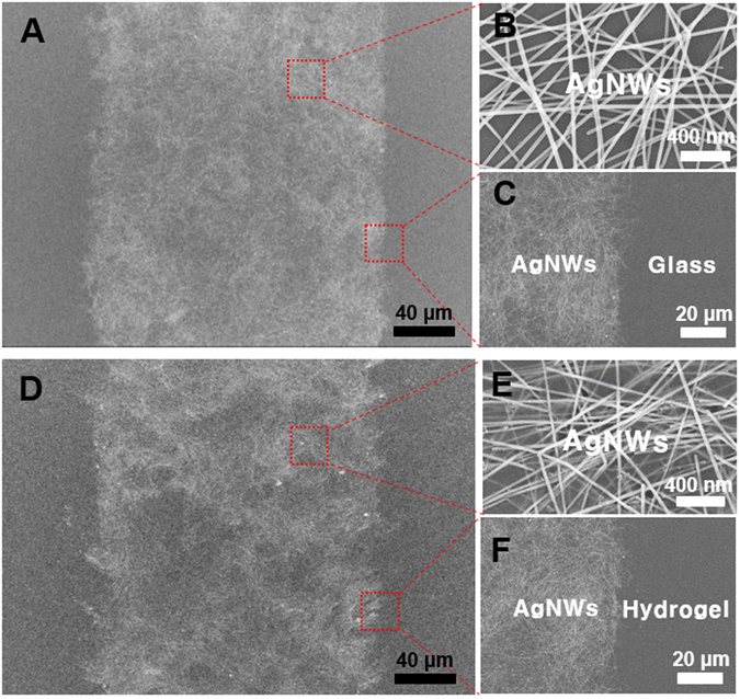
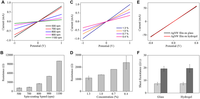
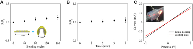
Hydrogel-based flexible microelectrodes have garnered considerable attention recently for soft bioelectronic applications. We constructed silver nanowire (AgNW) micropatterns on various substrates, via a simple, cost-effective, and eco-friendly method without aggressive etching or lift-off processes. Polyethylene glycol (PEG) photolithography was employed to construct AgNW patterns with various shapes and sizes on the glass substrate. Based on a second hydrogel gelation process, AgNW patterns on glass substrate were directly transferred to the synthetic/natural hydrogel substrates. The resultant AgNW micropatterns on the hydrogel exhibited high conductivity (ca. 8.40 × 10³ S cm-1) with low sheet resistance (7.51 ± 1.11 Ω/sq), excellent bending durability (increases in resistance of only ~3 and ~13% after 40 and 160 bending cycles, respectively), and good stability in wet conditions (an increase in resistance of only ~6% after 4 h). Considering both biocompatibility of hydrogel and high conductivity of AgNWs, we anticipate that the AgNW micropatterned hydrogels described here will be particularly valuable as highly efficient and mechanically stable microelectrodes for the development of next-generation bioelectronic devices, especially for implantable biomedical devices.


Conflict of interest statement

The authors declare that they have no competing interests.

Figures

Figure 1
Figure 1
Fabrication of AgNW patterns on various substrates via two consecutive solution-only processes. (A) Schematic illustration for fabrication of AgNW-based micropatterns on the hydrogel: (i) AgNW dispersion solution was spin-coated on a glass substrate; (ii) PEG photolithography process using UV light via a photomask; (iii) peeling off of the PEG hydrogel layer by detaching the silane-treated cover glass to construct AgNW patterns on the glass substrate; (iv) second gel precursor solution (agarose or polyethylene glycol, or polyacrylamide) was poured onto the AgNW-patterned glass, and a second gelation process was conducted; and (v) peeling off of the second gel layer and transfer of the AgNW patterns from the glass to the hydrogel substrate. (B) Photographs showing the procedure used to fabricate AgNW-based micropatterns: (a) peeling off of the PEG hydrogel layer by detaching the silane-treated cover glass; (b) AgNW micropatterns on the glass substrate; (c) peeling off of the second gel layer; and (d) transfer of the AgNW patterns from the glass to the hydrogel substrate.
Figure 2
Figure 2
Photographic and optical microscopic images of AgNW-based micropatterns with (A,B) dot of 500 μm diameter and (C,D) line of 200 μm width) on the (A,C) glass and (B,D) hydrogel.
Figure 3
Figure 3
FE-SEM images of (AC) AgNW-based micropatterns on a glass substrate before the pattern transfer process and (DF) AgNW-based micropatterns on a hydrogel substrate after pattern transfer process. The line pattern width is 200 μm.
Figure 4
Figure 4
Electrical properties of AgNW-based micropatterns (700 μm in width and 2 cm in length) was measured by attachment of the copper tape on both sides. (A) Current-voltage (I–V) characteristics of AgNW-based micropatterns at the different spin-coating speeds and (C) various concentrations of AgNWs dispersion solution. Spin-coating speeds from 500 to 1100 rpm were used to control the thickness of the micropatterns and concentration from 0.4 to 1.3% were used to control the quantity of AgNWs. Resistance of AgNW-based micropatterns on glass substrate as a function of (B) spin-coating speeds and (D) concentrations. (E) Current-voltage (I–V) characteristics of AgNW-based micropatterns on glass before direct transfer, and hydrogel substrate after direct transfer process. (F) Sheet resistance of AgNW-based micropatterns on glass and hydrogel with the different spin-coating speeds.
Figure 5
Figure 5
Mechanical flexibility or stability of AgNW-based micropatterns was measured by digital multi-tester device and compared to the initial value. (A) Bending test of AgNW-based micropatterns (700 μm in width and 2 cm in length) on PEG hydrogel. (B) Stability test of AgNW-based micropatterns on PEG hydrogel in DI water. (C) The I–V performance of the AgNW-micropatterns (500 μm in width, 2 cm in length) on hydrogel before bending and in bending state. The inset shows the LED emission with flexible AgNW-based micropatterns (500 μm in width and 2 cm in length) on agarose hydrogel.
Figure 6
Figure 6
(AD) Photograph images of AgNW-based micropatterns on various hydrogel or elastomer; (A) PEG (200 μm). (B) Polyacrylamide (PAAM) (200 μm) (C) Agarose (200 μm) and (D) PDMS (500 μm). Scale bar: 5 mm.
Figure 7
Figure 7
Fabrication of pressure-responsive device of two AgNW-microelectrodes on PEG hydrogel (1 mm on line pattern width) and tested the pressure response using hydrogel sandwich type. The inset shows that the experiments were conducted by applying pressure to the points where the line patterns with electrodes were engaged. The relative change of the resistance (RCR) graph of connected AgNW-microelectrode with different pressures (2.5, 4.5, 6.5, 8.5, and 10.5 kPa).

Similar articles

Cited by

References

    1. Ganin AY, et al. Bulk superconductivity at 38 K in a molecular system. Nat. Mater. 2008;7:367–371. doi: 10.1038/nmat2179. - DOI - PubMed
    1. Nam M-S, Ardavan A, Blundell SJ, Schlueter JA. Fluctuating superconductivity in organic molecular metals close to the Mott transition. Nature. 2007;449:584–587. doi: 10.1038/nature06182. - DOI - PubMed
    1. Edberg J, et al. Patterning and conductivity modulation of conductive polymers by UV light exposure. Adv. Funct. Mater. 2016;26:6950–6960. doi: 10.1002/adfm.201601794. - DOI
    1. Yoon S-S, Khang D-Y. Facile patterning of Ag nanowires network by micro-contact printing of siloxane. ACS Appl. Mater. Interfaces. 2016;8(35):23236–23243. doi: 10.1021/acsami.6b05909. - DOI - PubMed
    1. Shin SR, et al. Aligned carbon nanotube–based flexible gel substrates for engineering biohybrid tissue actuators. Adv. Funct. Mater. 2015;25:4486–4495. doi: 10.1002/adfm.201501379. - DOI - PMC - PubMed

Publication types