. 2017 May 25;7(1):2419.
doi: 10.1038/s41598-017-02541-2.

High-Gain Graphene Transistors with a Thin AlOx Top-Gate Oxide

Affiliations

High-Gain Graphene Transistors with a Thin AlOx Top-Gate Oxide

Erica Guerriero et al. Sci Rep. .

Abstract

The high-frequency performance of transistors is usually assessed by speed and gain figures of merit, such as the maximum oscillation frequency f max, cutoff frequency f T, ratio f max/f T, forward transmission coefficient S 21, and open-circuit voltage gain A v. All these figures of merit must be as large as possible for transistors to be useful in practical electronics applications. Here we demonstrate high-performance graphene field-effect transistors (GFETs) with a thin AlOx gate dielectric which outperform previous state-of-the-art GFETs: we obtained f max/f T > 3, A v > 30 dB, and S 21 = 12.5 dB (at 10 MHz and depending on the transistor geometry) from S-parameter measurements. A dc characterization of GFETs in ambient conditions reveals good current saturation and relatively large transconductance ~600 S/m. The realized GFETs offer the prospect of using graphene in a much wider range of electronic applications which require substantial gain.


Conflict of interest statement

The authors declare that they have no competing interests.

Figures

Figure 1
Figure 1
High-frequency GFET. (a) Optical image of one of the fabricated GFETs with the gate length L = 1.1 μm. Graphene stripe cannot be seen as it is completely covered by the contacts. (b) Schematic of the central part of the GFET. Source (S) and drain (D) contacts (Au; yellow) are separated by an underlap (length u) from the gate (G) contact (Al; red core), which is covered by an insulating layer (AlOx; gray shell). Width of graphene stripes Ws was 5, 20 and 50 μm. All GFETs had the same contact width (~50 μm) regardless of the stripe width. The channel width W=2Ws. (c) Scanning electron microscopy image of the central part of one the fabricated GFETs with the gate length L = 1 μm. The underlap is u=100 nm.
Figure 2
Figure 2
Output characteristics and small-signal conductances of the fabricated GFETs in ambient air. (a) Drain current ID as a function of VDS for different VGS in a GFET with W=10μm and L=1μm. The onset of saturation is at VDS=VGSV0 and it moves to larger |VDS| at larger |VGS|. (b) The transconductance gm and output conductance gd of the fabricated GFETs at the operating point at which they exhibit the largest voltage gain Av.
Figure 3
Figure 3
The highest gain in each of the fabricated GFETs at 10 MHz. (a) The open circuit voltage gain Av as a function of the gate length L. (b) The forward gain S21 as a function of W/L. The highest value of 12.5 dB was obtained for W=100μm and L=1.1μm. A W/L fit is suggested by the black line because S21 scales with gm and therefore with W/L.
Figure 4
Figure 4
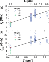
The largest values of the high-frequency transistor response parameters of each fabricated GFET as a function of gate length L. (a) The cuttof frequency fT and (b) maximum oscillation frequency fmax. A L1 fit is suggested by the black line in both plots.
Figure 5
Figure 5
The maximum oscillation frequency fmax as a function of the cutoff frequency fT of each fabricated GFET for different gate lengths L and channel widths W. The ratio fmax/fT varies between 1 and 3.

References

    1. Mayorov AS, et al. Micrometer-scale ballistic transport in encapsulated graphene at room temperature. Nano Lett. 2011;11:2396–2399. doi: 10.1021/nl200758b. - DOI - PubMed
    1. Novoselov KS, et al. Two-dimensional gas of massless dirac fermions in graphene. Nature. 2005;438:197–200. doi: 10.1038/nature04233. - DOI - PubMed
    1. Dorgan VE, Bae M-H, Pop E. Mobility and saturation velocity in graphene on SiO2 . Appl. Phys. Lett. 2010;97:082112. doi: 10.1063/1.3483130. - DOI
    1. Rizzi LG, et al. Cascading wafer-scale integrated graphene complementary inverters under ambient conditions. Nano Lett. 2012;12:3948–3953. doi: 10.1021/nl301079r. - DOI - PubMed
    1. Dean CR, et al. Boron nitride substrates for high-quality graphene electronics. Nature Nanotech. 2010;5:722–726. doi: 10.1038/nnano.2010.172. - DOI - PubMed

Publication types