. 2017 Apr 1;8(4):2522-2536.
doi: 10.1039/c6sc04474c. Epub 2016 Dec 16.

Metal halide perovskite nanomaterials: synthesis and applications

Affiliations

Metal halide perovskite nanomaterials: synthesis and applications

Son-Tung Ha et al. Chem Sci. .

Abstract

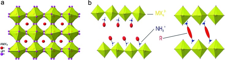
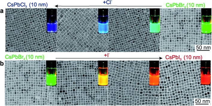
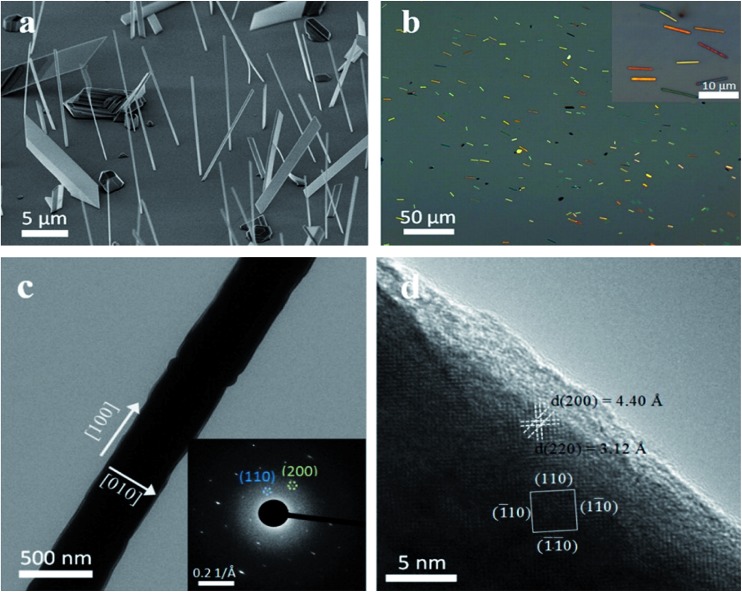
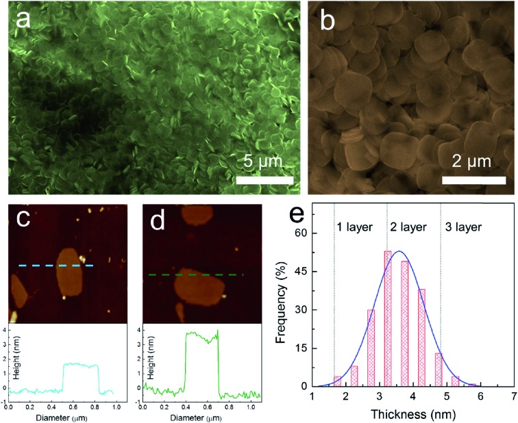
Nanomaterials refer to those with at least one dimension being at the nanoscale (i.e. <100 nm) such as quantum dots, nanowires, and nanoplatelets. These types of materials normally exhibit optical and electrical properties distinct from their bulk counterparts due to quantum confinement or strong anisotropy. In this perspective, we will focus on a particular material family: metal halide perovskites, which have received tremendous interest recently in photovoltaics and diverse photonic and optoelectronic applications. The different synthesis approaches and growth mechanisms will be discussed along with their novel characteristics and applications. Taking perovskite quantum dots as an example, the quantum confinement effect and high external quantum efficiency are among these novel properties and their excellent performance in applications, such as single photon emitters and LEDs, will be discussed. Understanding the mechanism behind the formation of these nanomaterial forms of perovskite will help researchers to come up with effective strategies to combat the emerging challenges of this family of materials, such as stability under ambient conditions and toxicity, towards next generation applications in photovoltaics and optoelectronics.


Figures

Fig. 1
Fig. 1. Structure of 3D and 2D perovskites: (a) structure of AMX3 3D perovskite; (b) structure of layered perovskites with (left) monoammonium (RNH3 +) or (right) diammonium (+H3N–R-NH3 +) organic cations.
Fig. 2
Fig. 2. (a) Schematic illustration of the reaction system and process for the LARP technique and typical optical image of the colloidal MAPbBr3 solution. (b) HRTEM image of MAPbBr3 colloidal NPs. (c) Optical absorption and PL spectra of perovskites with different halide components. (d) Digital image of the perovskite colloidal solutions in toluene under ambient light and an UV lamp, light emission from 438 to 660 nm. Reprinted with permission from ref. 17 and 45, copyright 2015, 2016 American Chemical Society.
Fig. 3
Fig. 3. Transmission electron microscopy (TEM) images of ∼10 nm CsPbX3 NCs after treatment with various quantities of (a) chloride and (b) iodide anions. The insets show the evolution of emission colors under an UV lamp. Reprinted with permission from ref. 50, copyright 2015, American Chemical Society.
Fig. 4
Fig. 4. (a) and (b) SEM images of CH3NH3PbI3 nanostructures. (c) PXRD patterns of as-grown CH3NH3PbX3 (X = I, Br, Cl) NWs. (d) TEM images of CsPbX3 NWs with various degrees of conversion with chloride and iodide anions. The insets show the evolution of emission color (UV excitation, λ = 365 nm) upon forming mixed-halide CsPb(Br/Cl)3 and CsPb(Br/I)3 NWs. HRTEM images of (e) Cl- and (f) I-exchange NWs. Reprinted with permission from ref. 15 and 74, copyright 2015, Nature Publishing Group and 2016, American Chemical Society.
Fig. 5
Fig. 5. (a) SEM image of PbI2 nanowires grown on the silicon substrate. (b) Optical microscopy image of CH3NH3PbI3 nanowires on the silicon substrate. Inset in (b) is the magnified image. (c) TEM and (d) HRTEM images of CH3NH3PbI3 nanowire. Inset in (c) is its corresponding SAED pattern. Reprinted with permission from ref. 39, copyright 2015, American Chemical Society.
Fig. 6
Fig. 6. Morphological characterizations of lead halide nano-platelets as-grown on a muscovite mica substrate: (a) optical (above) and SEM (below) images of lead halides: A, D: PbCl2; B, E: PbBr2; C, F: PbI2. (b) Schematic of the synthesis setup using a home-built vapor-transport system. (c) Thickness of PbI2 platelets before (images above data line) and after being converted to CH3NH3PbI3 (images below data line). Note that the color of the PbI2 platelets changes, corresponding to the change in thickness (as measured by AFM). (d) Optical properties of different lead halide perovskites (CH3NH3PbX3). Reprinted with permission from ref. 41, copyright 2014, Advance Optical Materials.
Fig. 7
Fig. 7. Synthesis of atomically thin 2D (C4H9NH3)2PbBr4 crystals. (A) Structural illustration of a single layer (C4H9NH3)2PbBr4 (blue balls, lead atoms; large orange balls, bromine atoms; red balls, nitrogen atoms; small orange balls, carbon atoms; H atoms were removed for clarity). (B) Optical image of the 2D square sheets. Scale bar, 10 mm. (C) AFM image and height profile of several single layers. The thickness is around 1.6 nm (T 0.2 nm). (D) AFM image and height profile of a double layer. The thickness is around 3.4 nm (T 0.2 nm). Reprinted from ref. 34, Copyright 2015, Science Publishing Group.
Fig. 8
Fig. 8. Synthesis of 2D ultrathin CsPbBr3 nanosheets: (a) low-magnification and (b) high-magnification SEM images. AFM image and height profile of (c) monolayer and (d) bilayer CsPbBr3 nanosheets with a thickness of 1.6 and 3.3 ± 0.2 nm, respectively. (e) Thickness distribution histograms for CsPbBr3 nanosheets prepared through solution-phase synthesis. Reprinted from ref. 79, copyright 2016, Advanced Materials.
Fig. 9
Fig. 9. (a) Colloidal perovskite CsPbX3 NCs (X = Cl, Br, I) solutions in toluene under an UV lamp (λ = 365 nm); (b) representative PL spectra (λ exc = 400 nm for all but 350 nm for CsPbCl3 nanocrystals). (c) Optical absorption and PL spectra of CsPbCl3, CsPbBr3, and CsPbI3 nanoplatelets. Inset: PL image of CsPbCl3, CsPbBr3, and CsPbI3 nanoplatelets. Reprinted with permission from ref. 40 and 49, copyright 2015, American Chemical Society and 2016, Advanced Material.
Fig. 10
Fig. 10. (a) Quantum-size effects in the absorption and emission spectra of 5–12 nm CsPbBr3 NCs. (b) Experimental versus theoretical (effective mass approximation, EMA) size dependence of the band gap energy. Reprinted with permission from ref. 49.
Fig. 11
Fig. 11. Optical lasing in lead halide perovskite nanoplatelets and nanowires. (a) Whisper-gallery mode lasing in a perovskite nanoplatelet cavity. (b) Fabry-Pérot lasing in a perovskite nanowire cavity. (c) Photoluminescence spectra of CsPbX3 (X = Cl, Br, I) nanoplatelets. (d) Wavelength tunability of perovskite lasing by changing the content of halide in CsPbX3 perovskite. Reprinted with permission from ref. 14, 15 and 40.
Fig. 12
Fig. 12. Low dimensional perovskite in LED applications. (a) LED from CH3NH3PbX3 quantum dots. (b) LED from CsPbX3 quantum dots. (c) LED from CH3NH3PbX3 nanoplatelets. Reprinted with permission from ref. 17, 90 and 91.

References

    1. Novoselov K. S. Science. 2004;306:666. - PubMed
    1. Song L. Nano Lett. 2010;10:3209. - PubMed
    1. Levendorf M. P. Nature. 2012;488:627. - PubMed
    1. Najmaei S. Nat. Mater. 2013;12:754. - PubMed
    1. Chhowalla M., Amaratunga G. A. Nature. 2000;407:164. - PubMed