

Rapid visualization of grain boundaries in monolayer MoS2 by multiphoton microscopy
- PMID: 28580960
- PMCID: PMC5465365
- DOI: 10.1038/ncomms15714
Rapid visualization of grain boundaries in monolayer MoS2 by multiphoton microscopy
Abstract
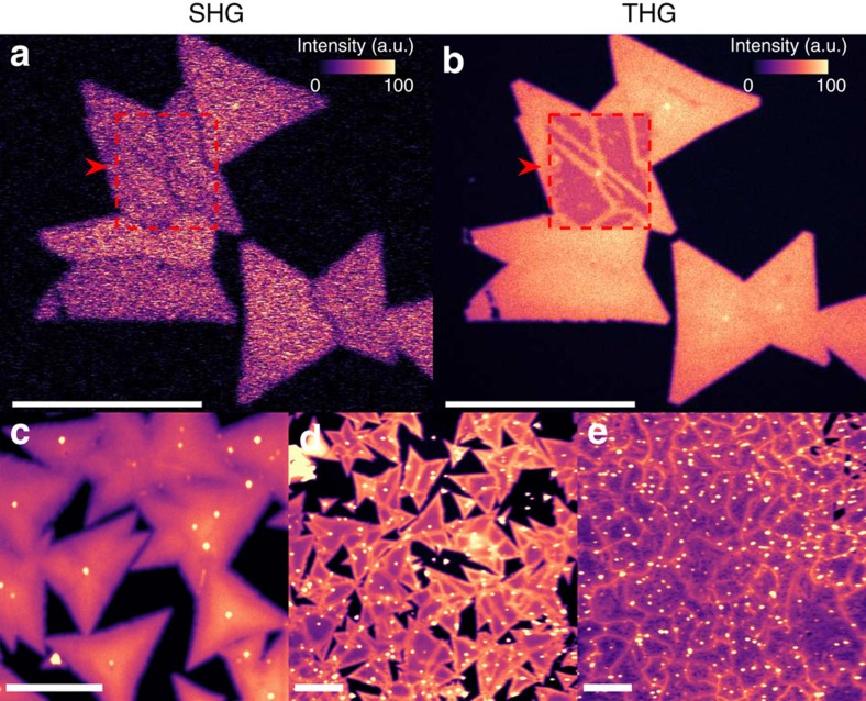
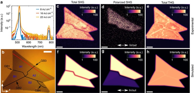
Grain boundaries have a major effect on the physical properties of two-dimensional layered materials. Therefore, it is important to develop simple, fast and sensitive characterization methods to visualize grain boundaries. Conventional Raman and photoluminescence methods have been used for detecting grain boundaries; however, these techniques are better suited for detection of grain boundaries with a large crystal axis rotation between neighbouring grains. Here we show rapid visualization of grain boundaries in chemical vapour deposited monolayer MoS2 samples with multiphoton microscopy. In contrast to Raman and photoluminescence imaging, third-harmonic generation microscopy provides excellent sensitivity and high speed for grain boundary visualization regardless of the degree of crystal axis rotation. We find that the contrast associated with grain boundaries in the third-harmonic imaging is considerably enhanced by the solvents commonly used in the transfer process of two-dimensional materials. Our results demonstrate that multiphoton imaging can be used for fast and sensitive characterization of two-dimensional materials.
Conflict of interest statement
The authors declare no competing financial interests.
Figures
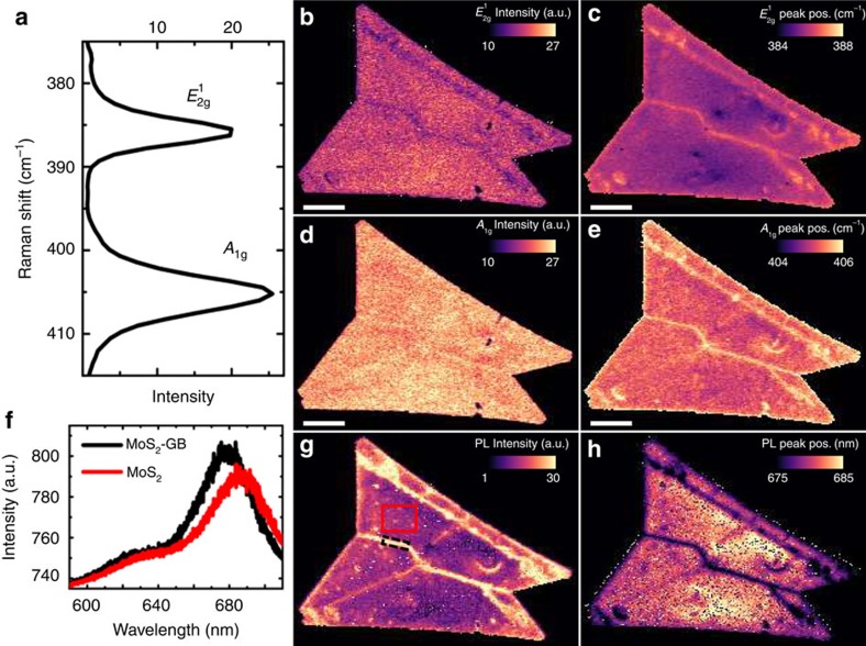
 peak, (c) centre position of
  peak, (d) intensity of A1g peak and (e) centre position of A1g peak, (f) PL spectra from the middle of the grain A1 (red curve, taken from the area marked with white line in g and from GB1 in the middle of the flake (black curve, taken from the area marked with a black dashed line in g. (g) PL intensity image of the 680 nm peak and (h) centre position of the 680 nm peak. Intensities and peak positions are acquired by Gaussian fitting. Scale bars, 10 μm. Colour scale bars are in CCD counts (Raman and PL intensities), in cm−1 (Raman peak positions) and in nm (PL peak position).
References
-
- Ferrari A. C. et al. Science and technology roadmap for graphene, related two-dimensional crystals, and hybrid systems. Nanoscale 7, 4598–4810 (2015). - PubMed
-
- Radisavljevic B., Radenovic A., Brivio J., Giacometti V. & Kis A. Single-layer MoS2 transistors. Nat. Nanotechnol. 6, 147–150 (2011). - PubMed
-
- Mak K. F., Lee C., Hone J., Shan J. & Heinz T. F. Atomically thin MoS2: a new direct-gap semiconductor. Phys. Rev. Lett. 105, 136805 (2010). - PubMed
-
- Splendiani A. et al. Emerging photoluminescence in monolayer MoS2. Nano Lett. 10, 1271–1275 (2010). - PubMed
Publication types
LinkOut - more resources
Full Text Sources
Other Literature Sources
