Review
. 2017 Jun 9:8:15756.
doi: 10.1038/ncomms15756.

Three-dimensional nanomagnetism

Affiliations
Review

Three-dimensional nanomagnetism

Amalio Fernández-Pacheco et al. Nat Commun. .

Abstract

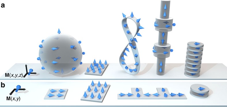
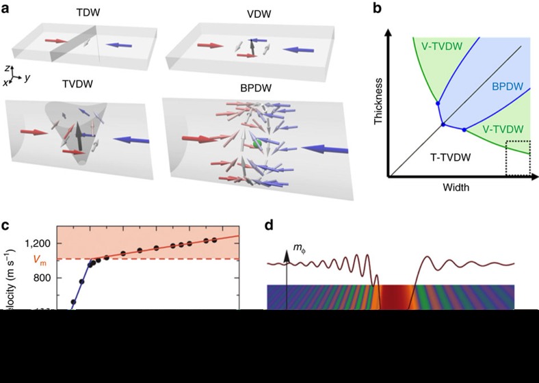
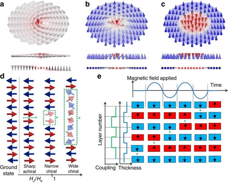
Magnetic nanostructures are being developed for use in many aspects of our daily life, spanning areas such as data storage, sensing and biomedicine. Whereas patterned nanomagnets are traditionally two-dimensional planar structures, recent work is expanding nanomagnetism into three dimensions; a move triggered by the advance of unconventional synthesis methods and the discovery of new magnetic effects. In three-dimensional nanomagnets more complex magnetic configurations become possible, many with unprecedented properties. Here we review the creation of these structures and their implications for the emergence of new physics, the development of instrumentation and computational methods, and exploitation in numerous applications.


Conflict of interest statement

The authors declare no competing financial interests.

Figures

Figure 1
Figure 1. Towards three-dimensional nanomagnetism.
Schematic view comparing some examples of geometries and magnetic configurations (indicated by blue arrows) for (a) 3D and (b) 2D nanomagnetism. The dependence of the magnetization M on spatial coordinates (black arrows) is indicated for both cases. New synthesis, characterization and computational methods have the potential to make the leap to 3D. The combination of more complex magnetic states and additional degrees of freedom in 3D nanomagnets leads to the emergence of new physical phenomena, which may find applications in multiple areas. (a) Examples of 3D nanomagnets, from left to right: magnetic sphere with vortex configuration. Magnetic thin film element with a skyrmion. Symmetry breaking is caused by bulk or interfacial Dzyaloshinskii-Moriya interaction. Möbius strip with perpendicular magnetization; a DW is present in the ground state due to the object's topology. Cylindrical NW with modulated diameter, with different magnetic configurations depending on the diameter. Antiferromagnetic (AF) superlattice (interlayers not shown for clarity) with a wide soliton in the middle. (b) Examples of 2D nanomagnets, from left to right: Single-domain magnet. Magnetic multi-layered element with perpendicular anisotropy. Nanostrip with protrusions for DW trapping. Bi-layered magnet with AF coupling due to indirect exchange via an interlayer (not shown for clarity).
Figure 2
Figure 2. New physical effects for DWs in 3D NWs and NTs.
(a) Types of DWs in nanostrips (transverse: TDW and vortex: VDW) and in 3D NWs (transverse-vortex: TVDW and Bloch-point: BPDW). The shaded areas represent the wall shape for the TDW and TVDW. BPDW: the green sphere represents a Bloch point. (b) Thickness-versus-width energy schematic phase diagram for DWs in NWs. These dimensions are relative to the dipolar exchange length in wires made of soft magnetic materials. In the white and green regions, TVDWs are typically observed, whereas in the blue area, BPDWs are energetically favourable. The region marked by dashed line represents the typical area referring to nanostrips, with widths much larger than thickness, where either TDW or VDW are observed. (c) Velocity of a DW with axial vortex configuration propagating in a NT as a function of external magnetic fields. Very high speeds are reached without experiencing a Walker breakdown. Two regimes with different mobilities are observed: the usual motion, described as Walker, and Magnonic (red region), above a critical velocity vm. The kink at the transition shows the change of mobility (effective mass) of the wall. (d) Snapshot of a simulation in the Magnonic regime, showing strong spin wave emission during DW propagation. The figure shows the azimuthal component of the magnetization (mϕ) in an unrolled NT, for an easier visualization. Panels (c) and (d) are reproduced from ref. with the permission of AIP Publishing.
Figure 3
Figure 3. Three-dimensional spin textures.
Schematics of (a) magnetic vortex, (b) (Neel) skyrmion and (c) chiral bubble, shown at different perspectives (oblique, side and top view). Whereas, the vortex nucleation is in general limited to nano- and micro-patterned planar magnets due to the interplay between Heisenberg exchange and magnetostatic contributions, skyrmions and chiral bubbles emerge in systems with broken inversion symmetry, for example, via antisymmetric Dzyaloshinskii–Moriya exchange interactions. (d) Macrospin model of an antiferromagnetic superlattice where the ground state corresponds to all spins antiparallel to each other. The introduction of a soliton divides the system in two anti-phases. The width and chirality (defined as the sense of rotation of the spins–clockwise or counter clockwise) of the soliton depends on the exchange (HJ)/anisotropy (Hu) field ratio of the system. The middle point and extension of the soliton in each case is marked by an asterisk and a green dashed rectangular area, respectively. Faded spins represent in-plane deviations from the easy axis. (e) Ratchet scheme for propagation of sharp achiral solitons. RKKY coupling and thickness change periodically between two values throughout the superlattice. The soliton, marked with an asterisk, moves synchronously under oscillating magnetic fields, propagating one step upwards every half field cycle.
Figure 4
Figure 4. Futuristic vision of an Internet-of-Things chip integrating 3D magnetic nanostructures.
The chip is comprised of a microfluidic channel with two types of magnetic nanoparticles flowing from a common reservoir. The motion of fluid is achieved by magnetic NWs acting as artificial cilia. After particle separation by chemical means, individual particles entering each channel are detected via a nanomembrane magnetic flexible sensor. An array of vertical soliton conduits acts as an ultra-high-density 3D storage device, with read/write operations taking place on the substrate. Neuromorphic computing processes are carried out by a dense array of interconnected NWs.

References

    1. Editorial. Memory with a spin. Nat. Nanotechnol. 10, 185–185 (2015). - PubMed
    1. Hoffmann A. & Bader S. D. Opportunities at the frontiers of spintronics . Phys. Rev. Appl. 4, 047001 (2015).
    1. McCray W. P. How spintronics went from the lab to the iPod. Nat. Nanotechnol. 4, 2–4 (2009). - PubMed
    1. Melzer M. et al.. Imperceptible magnetoelectronics. Nat. Commun. 6, 6080 (2015). - PMC - PubMed
    1. Makarov D., Melzer M., Karnaushenko D. & Schmidt O. G. Shapeable magnetoelectronics. Appl. Phys. Rev. 3, 011101 (2016).

Publication types