

Electrical gate control of spin current in van der Waals heterostructures at room temperature
- PMID: 28677673
- PMCID: PMC5504284
- DOI: 10.1038/ncomms16093
Electrical gate control of spin current in van der Waals heterostructures at room temperature
Abstract
Two-dimensional (2D) crystals offer a unique platform due to their remarkable and contrasting spintronic properties, such as weak spin-orbit coupling (SOC) in graphene and strong SOC in molybdenum disulfide (MoS2). Here we combine graphene and MoS2 in a van der Waals heterostructure (vdWh) to demonstrate the electric gate control of the spin current and spin lifetime at room temperature. By performing non-local spin valve and Hanle measurements, we unambiguously prove the gate tunability of the spin current and spin lifetime in graphene/MoS2 vdWhs at 300 K. This unprecedented control over the spin parameters by orders of magnitude stems from the gate tuning of the Schottky barrier at the MoS2/graphene interface and MoS2 channel conductivity leading to spin dephasing in high-SOC material. Our findings demonstrate an all-electrical spintronic device at room temperature with the creation, transport and control of the spin in 2D materials heterostructures, which can be key building blocks in future device architectures.
Conflict of interest statement
The authors declare no competing financial interests.
Figures
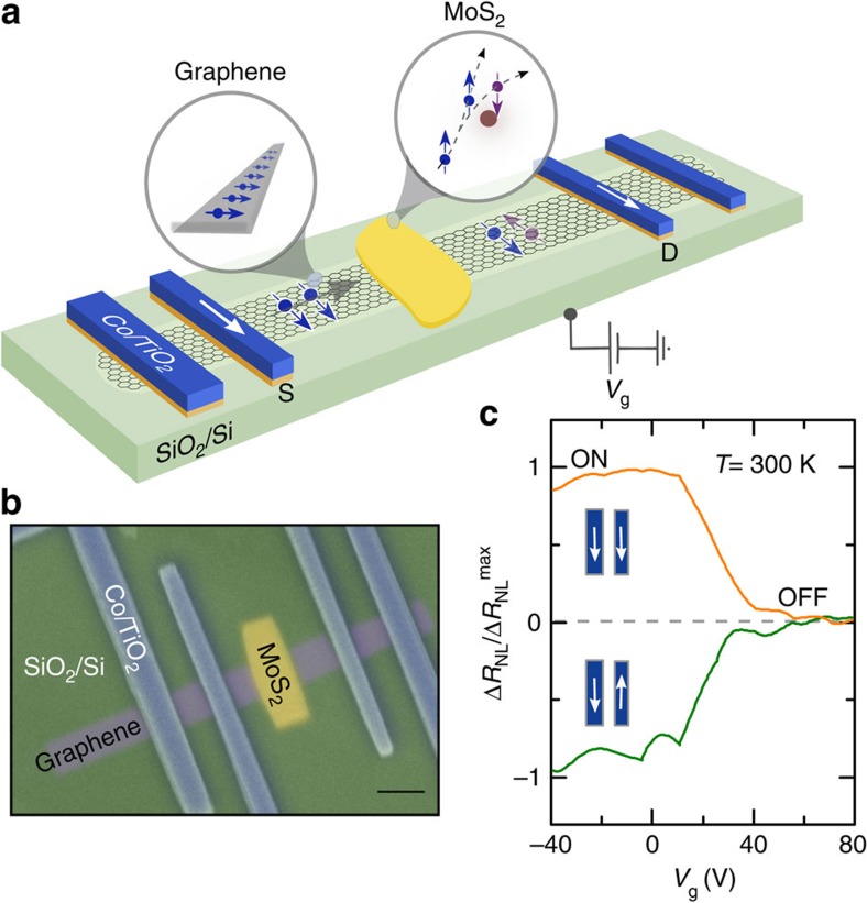
 normalized to the maximum value, showing transistor-like ON/OFF spin signal modulation at room temperature, for parallel and antiparallel magnetization alignments of source and drain.
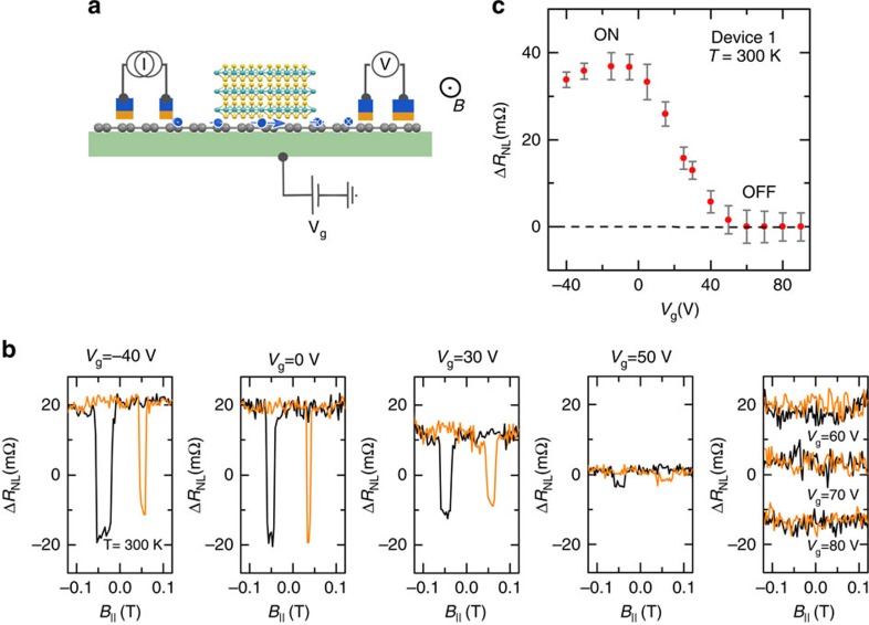
 measurements at 300 K by application of different gate voltages Vg. Measurements are performed at a constant current source of I=30 μA. A NL linear background (few μV) due to stray charge current is subtracted from the signal. (c) Modulation of spin-valve signal magnitude ΔRNL with gate voltage Vg, showing ON/OFF states at 300 K. The error bar is derived from the root mean square of the noise in the measured signal.
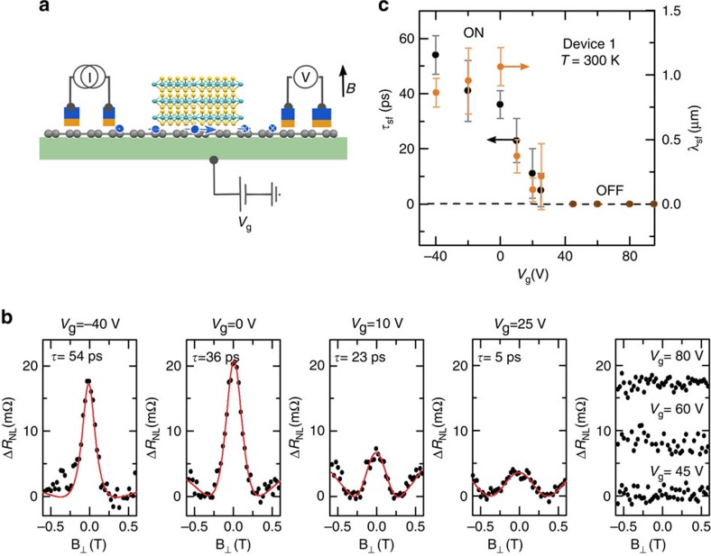
 . (b) NL Hanle spin signal
  measured at 300 K at different gate voltages. Measurements are performed at a constant current source of I=30 μA. The raw data points are fitted with equation (1) (red line) to extract spin lifetime τsf and diffusion length λsf. (c) The gate voltage Vg dependence of spin lifetime τsf (black) and diffusion length λsf (orange) at 300 K showing modulation of spin parameters from ON to OFF state. The error is derived from the error of the Hanle fit.
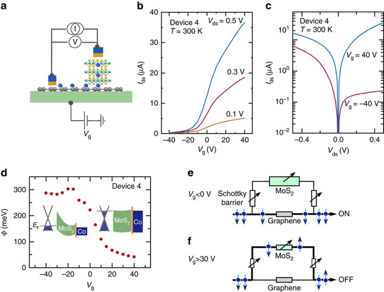
 . (d) Schottky barrier height Ф obtained for different Vg. Inset: Band structures at the MoS2/graphene interface for Vg<0 V and Vg>30 V. (e) Representative circuit diagram of the graphene and MoS2 parallel transport channels connected by Schottky barrier resistors in the heterostructure. At gate voltages Vg<0 V, the large Schottky barrier and high MoS2 resistance prevents spins from interacting with the high SOC MoS2 channel, resulting in a finite spin transport in graphene and corresponds to the spin-ON state. (f) At high gate voltages Vg>30 V, the reduced Schottky barrier and MoS2 channel resistance allows spins to tunnel into MoS2 and hence dephasing in the high-SOC material, resulting in the spin-OFF state.
References
-
- Žutić I., Fabian J. & Sarma S. Das. spintronics: fundamentals and applications. Rev. Mod. Phys. 76, 323–410 (2004).
-
- Awschalom D. D. & Flatté M. E. Challenges for semiconductor spintronics. Nat. Phys. 3, 153–159 (2007).
-
- Dash S. P., Sharma S., Patel R. S., de Jong M. P. & Jansen R. Electrical creation of spin polarization in silicon at room temperature. Nature 462, 491–494 (2009). - PubMed
-
- Ohno Y. et al. Electrical spin injection in a ferromagnetic semiconductor heterostructure. Nature 402, 790–792 (1999).
-
- Jansen R., Min B.-C. & Dash S. P. Oscillatory spin-polarized tunnelling from silicon quantum wells controlled by electric field. Nat. Mater. 9, 133–138 (2010). - PubMed
Publication types
LinkOut - more resources
Full Text Sources
Other Literature Sources
