. 2017 Jul 6:8:16025.
doi: 10.1038/ncomms16025.

Ballistic superconductivity in semiconductor nanowires

Affiliations

Ballistic superconductivity in semiconductor nanowires

Hao Zhang et al. Nat Commun. .

Erratum in

  • Author Correction: Ballistic superconductivity in semiconductor nanowires.
    Zhang H, Gül Ö, Conesa-Boj S, Nowak MP, Wimmer M, de Vries FK, van Veen J, de Moor MWA, Bommer JDS, van Woerkom DJ, Car D, Plissard SR, Bakkers EPAM, Quintero-Pérez M, Cassidy MC, Koelling S, Goswami S, Watanabe K, Taniguchi T, Kouwenhoven LP. Zhang H, et al. Nat Commun. 2025 Mar 12;16(1):2459. doi: 10.1038/s41467-025-57863-x. Nat Commun. 2025. PMID: 40075088 Free PMC article. No abstract available.

Expression of concern in

  • Editorial Expression of Concern: Ballistic superconductivity in semiconductor nanowires.
    Zhang H, Gül Ö, Conesa-Boj S, Nowak MP, Wimmer M, de Vries FK, van Veen J, de Moor MWA, Bommer JDS, van Woerkom DJ, Car D, Plissard SR, Bakkers EPAM, Quintero-Pérez M, Cassidy MC, Koelling S, Goswami S, Watanabe K, Taniguchi T, Kouwenhoven LP. Zhang H, et al. Nat Commun. 2025 Apr 3;16(1):3185. doi: 10.1038/s41467-025-58136-3. Nat Commun. 2025. PMID: 40180910 Free PMC article. No abstract available.

Abstract

Semiconductor nanowires have opened new research avenues in quantum transport owing to their confined geometry and electrostatic tunability. They have offered an exceptional testbed for superconductivity, leading to the realization of hybrid systems combining the macroscopic quantum properties of superconductors with the possibility to control charges down to a single electron. These advances brought semiconductor nanowires to the forefront of efforts to realize topological superconductivity and Majorana modes. A prime challenge to benefit from the topological properties of Majoranas is to reduce the disorder in hybrid nanowire devices. Here we show ballistic superconductivity in InSb semiconductor nanowires. Our structural and chemical analyses demonstrate a high-quality interface between the nanowire and a NbTiN superconductor that enables ballistic transport. This is manifested by a quantized conductance for normal carriers, a strongly enhanced conductance for Andreev-reflecting carriers, and an induced hard gap with a significantly reduced density of states. These results pave the way for disorder-free Majorana devices.


Conflict of interest statement

The authors declare no competing financial interests.

Figures

Figure 1
Figure 1. TEM analysis of a typical device.
(a) Top-view, false-colour electron micrograph of device A. Scale bar, 1 μm. Normal metal contact is Cr/Au (10 nm/125 nm) and superconducting contact is NbTi/NbTiN (5 nm/85 nm). Contact spacing is ∼100 nm. (b) Device schematic and measurement setup. (c) Low-magnification high-resolution TEM (HRTEM) cross-sectional image from the device (see Methods). Scale bar, 50 nm. The cut was performed perpendicular to the nanowire axis, indicated by the dark bar in a. InSb nanowire exhibits a hexagonal cross-section surrounded by {220} planes. The NbTiN on the pre-layer NbTi crystallizes as cone-like elongated grains, indicated by the thin black lines. Corresponding fast Fourier transform confirms the polycrystalline character of the NbTiN region (Supplementary Fig. 2b). (d) HRTEM image near the interface (red square in c) shows that our cleaning procedure only minimally etches the wire and the InSb crystalline properties are preserved after the deposition. Scale bar, 5 nm. (e) Energy-dispersive X-ray (EDX) compositional map of the device cross-section. Scale bar, 50 nm. (f) EDX line scan taken across the interface as indicated by the red arrow in e. The sulfur content is multiplied by 5 for clarity. The system is oxygen and argon free (contact deposition is performed in an Ar plasma environment).
Figure 2
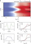
Figure 2. Ballistic transport at zero magnetic field.
(a) Differential conductance, dI/dV, as a function of bias voltage, V, and gate voltage, Vgate for device B. (b) Vertical line cut from a in tunnelling regime (green trace, gate voltage=−12 V). (c) Vertical line cut from a on the conductance plateau (blue trace, gate voltage=−5.9 V). (d) Horizontal line cuts from a showing above-gap (Gn, black, |V|=2 mV) and subgap (Gs, red, V=0 mV) conductance. (e) Above-gap (black) and subgap (red) conductance for device C, where Gs enhancement reaches 1.9 × 2e2/h.
Figure 3
Figure 3. Theoretical simulation.
(a) Theoretical model (top): a cylindrical nanowire (black, grey, white) with length LN+L (100 nm+800 nm), where the latter part is partially coated by a superconductor leaving the bottom surface uncovered. (Scheme shows L=100 nm for clarity.) The wire radius R is 40 nm and the superconducting film has a thickness Rs=10 nm. (Our wire radius varies from device to device between 30 and 50 nm, and we have confirmed that our simulations give similar results within this range.) The wire is terminated from both sides with infinite leads (pink). Front lead is normal, back lead is normal/superconductor. Each little circle represents a three-dimensional mesh site with a size of 7 nm. White circles depict a potential barrier with a width W=60 nm in the uncovered wire section forming a quantum point contact (QPC). Grey circles represent the smoothness of the barrier which is set to 5 nm. Experimental geometry (bottom): cross-sectional schematic shows the nanowire (NW), the normal contact (N) and the superconducting contact (S). Superconductivity is induced in the nanowire section underneath the superconducting contact. Transport is ballistic through a proximitized wire section, whose length far exceeds LN, the length of the non-covered wire between the contacts. (b) Numerical simulation for devices with different mean free paths (see Supplementary Fig. 5). Black trace is for Gn corresponding to a mean free path 10 μm, the rest are for Gs corresponding to a mean free path ranging from 1 μm (pink) to 20 μm (blue). (c) Above-gap (black) and subgap (red) conductance for device D. (d,e) Comparison between the measurement (device C) and the simulation of a ballistic device with le=10 μm. The induced superconducting gap edges for higher subbands, visible in the simulation as four symmetric peaks outside the gap around V ∼±1 mV, are not observed in the experiment (see Methods for details).
Figure 4
Figure 4. Hard gap and Andreev transport.
(a) Above-gap (black) and subgap (blue) conductance for device E. Red curve is a theory prediction based on single channel Andreev reflection, agreeing perfectly with experimental data without any fitting parameter up to the dip on the right side of the plateau where the second channel starts conducting. (b,c) Five typical gap traces corresponding to the five colour bars indicated in d plotted on a linear and logarithmic scale. The subgap conductance is suppressed by a factor up to 50 for the lowest conductance (red trace). (d) Subgap conductance Gs as a function of above-gap conductance Gn for device A. Red curve is the theory prediction assuming only Andreev processes. Inset shows Gs versus Gn taken at different magnetic fields.

References

    1. Read N. & Green D. Paired states of fermions in two dimensions with breaking of parity and time-reversal symmetries and the fractional quantum Hall effect. Phys. Rev. B 61, 10267 (2000).
    1. Kitaev A. Y. Unpaired Majorana fermions in quantum wires. Phys. Usp. 44, 131–136 (2001).
    1. Fu L. & Kane C. L. Superconducting proximity effect and Majorana fermions at the surface of a topological insulator. Phys. Rev. Lett. 100, 096407 (2008). - PubMed
    1. Lutchyn R. M., Sau J. D. & Das Sarma S. Majorana fermions and a topological phase transition in semiconductor-superconductor heterostructures. Phys. Rev. Lett. 105, 077001 (2010). - PubMed
    1. Oreg Y., Refael G. & von Oppen F. Helical liquids and Majorana bound states in quantum wires. Phys. Rev. Lett. 105, 177002 (2010). - PubMed

Publication types