. 2017 Jul 12;3(7):e1700234.
doi: 10.1126/sciadv.1700234. eCollection 2017 Jul.

Electrochemical electron beam lithography: Write, read, and erase metallic nanocrystals on demand

Affiliations

Electrochemical electron beam lithography: Write, read, and erase metallic nanocrystals on demand

Jeung Hun Park et al. Sci Adv. .

Abstract

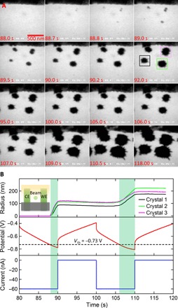
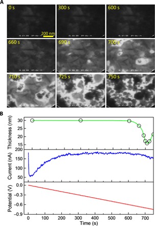
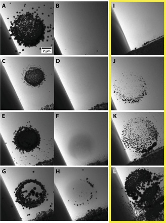
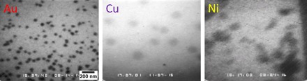
We develop a solution-based nanoscale patterning technique for site-specific deposition and dissolution of metallic nanocrystals. Nanocrystals are grown at desired locations by electron beam-induced reduction of metal ions in solution, with the ions supplied by dissolution of a nearby electrode via an applied potential. The nanocrystals can be "erased" by choice of beam conditions and regrown repeatably. We demonstrate these processes via in situ transmission electron microscopy using Au as the model material and extend to other metals. We anticipate that this approach can be used to deposit multicomponent alloys and core-shell nanostructures with nanoscale spatial and compositional resolutions for a variety of possible applications.


Figures

Fig. 1
Fig. 1. Electron beam–induced deposition process of Au nanocrystals under electrochemical control.
(A) Time sequence of bright-field TEM images obtained in a liquid cell showing the size evolution of one Au nanocrystal (among seven growing within the field of view) during pulsed galvanostatic electrochemical deposition in 0.1 M HCl. The electron dose rate is 46 e2·s. The full sequence is shown in movie S1, and additional images of the whole irradiated area are shown in fig. S1A. (B) Driving current (−60 nA in 10-s pulses), the resulting measured potential, and the radius versus time of three of the nanocrystals. The black, green, and magenta boxes shown in (A) at 92 s correspond to crystals 1, 2, and 3 in (B), respectively. Growth did not occur during the first four current pulses, only starting when the potential went below a threshold value Vth ~ −0.73 V. Note that when the current is off, the radii decrease slightly under the beam. Light green shading indicates times at which nanocrystal growth was observed, consistently at potentials below −0.70 V. The smallest observable nanocrystal is around 25 nm in diameter (second image).
Fig. 2
Fig. 2. Electrochemical control of Au ion supply via the oxidation and dissolution of the Au CE.
(A) Microstructural evolution of the Au CE during linear sweeping potentiometry. A series of bright-field TEM images was recorded near the center of a 30-nm-thick Au electrode in 0.1 M HCl as the potential was swept from 0 to 0.75 V at 1 mV/s. The beam conditions were constant at a dose rate of 46 e2·s. The complete data set is shown in movie S2. (B) Applied potential, measured current, and remaining thickness of Au (estimated from the transmitted brightness) are plotted as a function of time. If measured over the interval between −0.66 and −0.73 V, this thickness change corresponds to the release of 2 × 10¹⁰ Au ions/s over the area of the electrode. The times of the images in (A) are indicated with open circles (○). The apparent increase in thickness after 710 s is caused by electron beam–induced redeposition of Au in areas where the electrode has been removed. All images were obtained with the same field of view.
Fig. 3
Fig. 3. Series of bright-field liquid cell TEM images showing sequential writing and erasing of Au nanocrystals.
The images were obtained after writing or erasing was complete, spreading the beam to image an area larger than the area irradiated during the experiment. (A to H) Image pairs showing writing (A, C, E, and G) at a dose rate 46 e2·s and a current or potential described below, followed by etching (B, D, F, and H) at a higher dose rate, dc ~ 260 e2·s, and zero applied potential. (A) First writing: Nanocrystals formed after 14 deposition cycles, each consisting of 5 s at −60 nA and 5 s at 0 nA. (B) Erasing of the first deposits at 0 nA. (C) Second writing: Nanocrystals formed after seven deposition cycles, each consisting of 5 s at −60 nA and 5 s at 0 nA. (D) Erasing of the second deposits at 0 nA. (E) Third writing using the stepped potential shown in fig. S2A, scanning from −0.3 to −0.8 V with 10-s 0.05-V steps. (F) Erasing of third deposits at 0 V. (G) Fourth writing using the potential shown in fig. S2B, −0.75 V for 10 s followed by −0.65 V for 10 s. (H) Erasing of the fourth deposits at 0 V. (I to L) Morphologies obtained using different modulations of a −60-nA current. Current was applied for 2 s (I), 3 s (J), 4 s (K), and 6 s (L) at −60 nA, respectively, followed by 2 s at 0 nA. Circular shadows in (F) and (H) are due to radiation damage of the silicon nitride windows during the long experiment. Additional images from the sequences are shown in figs. S3 and S4. All images were obtained with the same field of view.
Fig. 4
Fig. 4. Electrochemical + radiolytic formation of Au, Cu, and Ni nanocrystals.
All growths occur in 0.1 M HCl during linear potential sweeping at 1 mV/s for Au, 5 mV/s for Cu, and 1 mV/s for Ni. The measured onset potentials are shown in table S1 and other electrochemical parameters are shown in fig. S7. All images are obtained at the same field of view.

Similar articles

Cited by

References

    1. I. Utke, S. Moshkalev, P. Russell, Eds., Nanofabrication Using Focused Ion and Electron Beams - Principles and Applications (Oxford Univ. Press, 2012).
    1. Xia Y., Xiong Y., Lim B., Skrabalak S. E., Shape-controlled synthesis of metal nanocrystals: Simple chemistry meets complex physics? Angew. Chem. Int. Ed. 48, 60–103 (2009). - PMC - PubMed
    1. Mijatovic D., Eijkel J. C. T., van den Berg A., Technologies for nanofluidic systems: Top-down vs. bottom-up—A review. Lab Chip 5, 492–500 (2005). - PubMed
    1. Vieu C., Carcenac F., Pépin A., Chen Y., Mejias M., Lebib A., Manin-Ferlazzo L., Couraud L., Launois H., Electron beam lithography: Resolution limits and applications. Appl. Surf. Sci. 164, 111–117 (2000).
    1. Kim C.-S., Ahn S.-H., Jang D.-Y., Review: Developments in micro/nanoscale fabrication by focused ion beams. Vacuum 86, 1014–1035 (2012).

Publication types