. 2017 Jul 25;7(1):6360.
doi: 10.1038/s41598-017-06957-8.

Strain Balanced AlGaN/GaN/AlGaN nanomembrane HEMTs

Affiliations

Strain Balanced AlGaN/GaN/AlGaN nanomembrane HEMTs

Tzu-Hsuan Chang et al. Sci Rep. .

Abstract

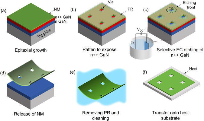
Single crystal semiconductor nanomembranes (NM) are important in various applications such as heterogeneous integration and flexible devices. This paper reports the fabrication of AlGaN/GaN NMs and NM high electron mobility transistors (HEMT). Electrochemical etching is used to slice off single-crystalline AlGaN/GaN layers while preserving their microstructural quality. A double heterostructure design with a symmetric strain profile is employed to ensure minimal residual strain in freestanding NMs after release. The mobility of the two-dimensional electron gas (2DEG), formed by the AlGaN/GaN heterostructure, is noticeably superior to previously reported values of many other NMs. AlGaN/GaN nanomembrane HEMTs are fabricated on SiO2 and flexible polymeric substrates. Excellent electrical characteristics, including a high ON/OFF ratio and transconductance, suggest that III-Nitrides nanomembranes are capable of supporting high performance applications.


Conflict of interest statement

The authors declare that they have no competing interests.

Figures

Figure 1
Figure 1
Fabrication procedure of III-Nitride NM. (a) Epitaxial growth of NM to be lift-off with an underneath n++ GaN layer, (b) photolithograph and dry etching to expose n++ GaN sidewalls with arrays of vias, (c) selective undercut etching of n++ GaN by electrochemical etching, (d) separation of NM from epitaxial wafer after full undercut, (e) removal of photoresist and cleaning the NM, (f) transfer the freestanding NM onto a host substrate.
Figure 2
Figure 2
(a) An AlGaN/GaN/AlGaN NM on SiO2/Sapphire, (b) Microscopy image of a NM on SiO2/Si with diagonal spacing of 100 µm, (c) and (d) SEM and AFM images of the Ga-polar surface of a NM, respectively.
Figure 3
Figure 3
(a) The Raman spectrum of DH NM with the exciting laser spot on the NM and on the edge of NM. (b) SEM image of an N-polar NM with diagonal via spacing of 25 µm (c) Spatial mapping of intensity ratio of the A1 (TO) to E2 (high) peak. The scanning area is 60 × 60 µm2, indicated by red square in (b).
Figure 4
Figure 4
High resolution X-ray diffraction of DH NM on SiO2/Si. (a) The (105) reciprocal space mapping. (b) (002) ω/2θ scan. (c) (002) rocking curve of GaN. (d) (102) rocking curve of GaN.
Figure 5
Figure 5
NM HEMT on SiO2/Si. (a) The SEM image of a device with two separate 25 µm × 4 µm channels. Electrodes are colored and labeled. I-V is measured with one channel. (b) IG-VG of the Schottky gate in linear (black) and logarithmic (red) scales. (c) ID-VD at different gate bias from −3 V to 2 V, with step of 0.5 V. (d) Transfer characteristics (ID-VG) with VD of 4 V (red curve). Measured transconductance gm is also shown in black.
Figure 6
Figure 6
NM HEMT on polyester substrate. (a) Photo of NM HEMTs on PET with bend radius of about 3 cm. (b) NM HEMT microscopy image with back illumination, showing the transparency of the NM. (c) Front side of active region. (d) Backside of active region. (e) ID-VD with gate bias from −3 V to 2 V, with step of 0.5 V. (f) ID-VG with VD of 4 V.

References

    1. Ahn J-H, et al. Heterogeneous Three-Dimensional Electronics by Use of Printed Semiconductor Nanomaterials. Science. 2006;314:1754–1757. doi: 10.1126/science.1132394. - DOI - PubMed
    1. Ko H, et al. Ultrathin compound semiconductor on insulator layers for high-performance nanoscale transistors. Nature. 2010;468:286–289. doi: 10.1038/nature09541. - DOI - PubMed
    1. Carlson A, Bowen AM, Huang Y, Nuzzo RG, Rogers JA. Transfer Printing Techniques for Materials Assembly and Micro/Nanodevice Fabrication. Adv. Mater. 2012;24:5284–5318. doi: 10.1002/adma.201201386. - DOI - PubMed
    1. Sun Y, Rogers JA. Inorganic Semiconductors for Flexible Electronics. Adv. Mater. 2007;19:1897–1916. doi: 10.1002/adma.200602223. - DOI
    1. Wang C, et al. Self-Aligned, Extremely High Frequency III–V Metal-Oxide-Semiconductor Field-Effect Transistors on Rigid and Flexible Substrates. Nano Lett. 2012;12:4140–4145. doi: 10.1021/nl301699k. - DOI - PubMed

Publication types