Review
. 2017 Jul 27;17(8):1726.
doi: 10.3390/s17081726.

Metamaterials and Metasurfaces for Sensor Applications

Affiliations
Review

Metamaterials and Metasurfaces for Sensor Applications

Yohan Lee et al. Sensors (Basel). .

Abstract

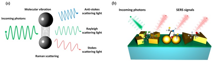
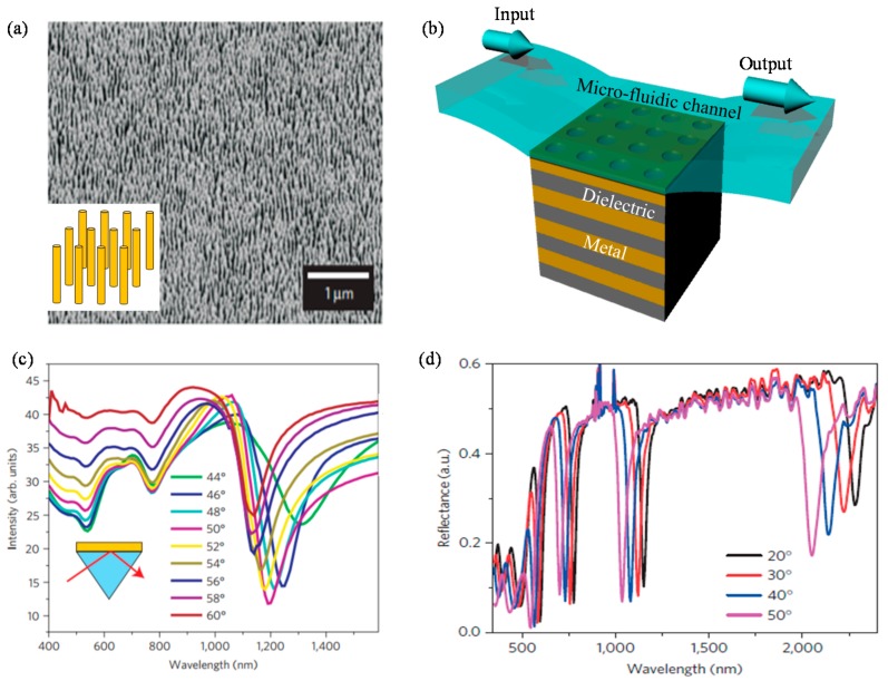
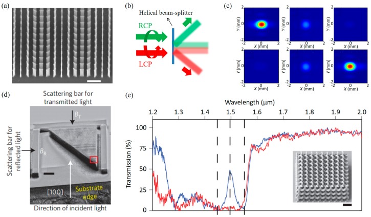
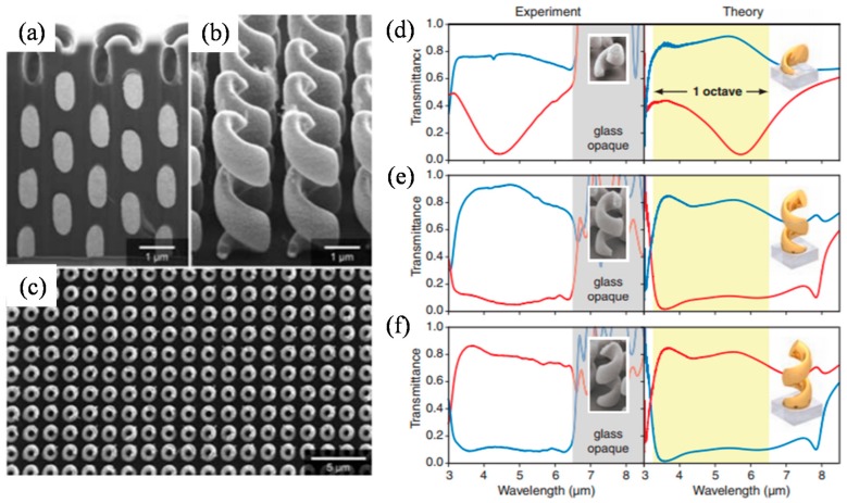
Electromagnetic metamaterials (MMs) and metasurfaces (MSs) are artificial media and surfaces with subwavelength separations of meta-atoms designed for anomalous manipulations of light properties. Owing to large scattering cross-sections of metallic/dielectric meta-atoms, it is possible to not only localize strong electromagnetic fields in deep subwavelength volume but also decompose and analyze incident light signal with ultracompact setup using MMs and MSs. Hence, by probing resonant spectral responses from extremely boosted interactions between analyte layer and optical MMs or MSs, sensing the variation of refractive index has been a popular and practical application in the field of photonics. Moreover, decomposing and analyzing incident light signal can be easily achieved with anisotropic MSs, which can scatter light to different directions according to its polarization or wavelength. In this paper, we present recent advances and potential applications of optical MMs and MSs for refractive index sensing and sensing light properties, which can be easily integrated with various electronic devices. The characteristics and performances of devices are summarized and compared qualitatively with suggestions of design guidelines.

Keywords: biosensor; light analysis; metamaterial; metasurface; polarimetry; refractive index sensing; spectroscopy.


Conflict of interest statement

The authors declare no conflict of interest.

Figures

Figure 1
Figure 1
(a) The principle of Raman scattering; (b) Illustration of SERS sensing. Roughened metal surface or metallic nanostructures can enhance Raman signals and they can be applied to biological and chemical sensing.
Figure 2
Figure 2
(a) A schematic illustration of SRR. Structural parameters are described. Magnetic field is generated along z-axis when x-polarized incidence is coming along z-axis; (b) Hz-field profile on resonance. It shows the generation of current loops (black arrows). The resonance conditions are as follow: λ = 1300 nm, Sx = Sy = 320 nm, Px = 504 nm, Py = 480 nm, w = 80nm, t = 30 nm, b = 128 nm; (c) A schematic illustration of chemical sensor of 2-naphtalenethiol using MM; (d) Raman spectra of 2-naphtalenethiol on various substrate environments; (e) Transmission spectra with and without 2-naphtalenethiol. The inset is the zoom-in view of the spectra around the magnetic resonance mode. (f) Schematic configuration of vis-NIR SRR MMs for detection and identification of biomolecules. This SRR sensor was designed to functionalize with AS1411, an effective anticancer drug. Parts (ce) are reprinted with permission from Reference [84]. Copyright (2011) American Chemical Society. Part (f) is reprinted with permission from Reference [85]. Copyright (2013) American Chemical Society.
Figure 3
Figure 3
(a) Schematic configuration of nanodisk-based MM; Structural parameters are described. (b) Absolute value of Hz-field profile on resonance. It shows the generation of current loops (black arrows). The resonance conditions are as follow: λ = 879 nm, D = 130 nm, h = 30 nm, t = 30nm, Px = 580 nm, Py = 300 nm; (c) Schematic illustration of double-resonances gold nanodisk array substrate (left panel) and its SEM image (right panel); (d) SERS spectra on double-resonances. The diameter changes from 100 to 143 nm (black to purple); (e) Reflectance spectra corresponding to (d). Parts (ce) are reprinted from Reference [87], with the permission of AIP Publishing.
Figure 4
Figure 4
(a) Schematic illustration of classical coupled oscillators. Two oscillators are linked with harmonic potential; (b) Real values of x2 in Equation (2) are plotted. Each curve refers to cases when a2 = 0 (red line) and a2 = 1 (blue line), respectively. To compare with single oscillator system, Lorentzian line-shapes of single cavity 1 (green dashed line) and 2 (black dashed line) with Q-factor of 10 are plotted, too (ω1 = 1, ω2 = 1.1, γ1 = 0.1, γ2 = 0.01, κ = 0.25).
Figure 5
Figure 5
Calculated spectra of quadrumers in different dielectric environments. (a) The dip of Fano resonance is highly sensitive to the surrounding; (b) Scattering spectra of a quadrumer embedded in environments of different index of refraction; (c) The calculated figure of merit. The inset shows the calculated sensitivity to be 647 nm/RIU. Reprinted with permission from Reference [94]. Copyright (2010) American Chemical Society.
Figure 6
Figure 6
(a) Planar MMs with asymmetric split copper rings. The dashed boxes indicate unit-cell structure; (b) Quality factor of “trapped-mode” resonance as a function of the particle asymmetry γ, defined as the relative difference of the arcs’ lengths; (c) Schematic representations of proteins’ mono- and bilayers binding to the metal surface and the equivalent dielectric model; (d) Experimental spectra before (dashed lines) and after (solid lines) binding of IgG antibodies to three different Fano-resonant asymmetric MMs substrates immobilized by the protein A/G. Reprinted (a,b) with permission from Reference [115]. Copyright (2007) by the American Physics Society. Reprinted (c,d) by permission form Macmillan Publishers Ltd.: (Nature Materials) (Reference [123]), copyright (2012).
Figure 7
Figure 7
(a) Side-view SEM image of gold mushroom MMs. The scale bar is 200 nm; (b) Reflectance spectra of the gold mushroom array structure immersed in glycerine at the incidence angle of 33.3°; (c) Normalized relfectance spectra for D1 in the spectral region indicated with the dashed box in (b). The refractive index changes from 1.333 to 1.417 (black to pink); (d) A schematic configuration, depicting the geometrical parameters of the capped gold nanoslits, as well as the direction of the TM-polarized incidence with E and K vectors; (e) Intensity spectra of the capped gold nanoslit with a 650-nm period in carious water/glycerin mixtures for a normally-incident TM-polarized wave; (f) Measured intensity spectra for different surface conditions. Reprinted by permission from Macmillan Publishers Ltd.: (Nature Communications) Reference [128], copyright (2013).
Figure 8
Figure 8
Schemes of basic HMM types whose optic axes are lying in: (a) horizontal (x-direction); and (b) perpendicular (y-direction) directions; (c,d) refer to isofrequency dispersion surfaces in the normalized momentum space for HMMs with (a,b) structures. Analytic expressions of plots in (c,d) are Equations (3) and (4).
Figure 9
Figure 9
(a) Scanning electron microscopy image of standing gold nanorods assembly with subwavlength spacings made by A. V. Kabashin et al. [135]. The inset figure presents magnified scheme of standing gold nanorods; (b) Scheme of the grating coupled HMM consists of alternatively stratified metal nanolayers and dielectric nanolayers demonstrated by Sreekanth et al. [136]; (c) Attenuated total reflection (ATR) spectra for nine different incidence angles when nanorod HMM of (a) is located in water environment (n = 1.33); (d) ATR spectra of the grating coupled HMM depicted in (b) for four different incidence angles. The legends in (c,d) denote the incidence angles. Reprinted by permission from Macmillan Publishers Ltd.: (Nature Materials) (Reference [135]), copyright (2009) and (Nature Materials) (Reference [136]), copyright (2016).
Figure 10
Figure 10
The simplest schemes for refractive index sensing with an HPG MS and tunable refractions when an input beam is incident from (a) a substrate side and (b) a superstrate analyte side. nanal, nsub, θi, and θt denote refractive index of analyte layer, refractive index of substrate, incident angle of an input beam, and refraction angle of a transmitted beam. The yellow patterns represent an arbitrary HPG MS.
Figure 11
Figure 11
(a) SEM image; and (b) schematic illustration of helical beam-splitter demonstrated by M. Khorasaninejad and K. B. Crozier [156]. Scale bar, 1 μm; (c) Captured CCD images of diffraction. The first and second rows present LCP and RCP cases. The first, second, and third columns present −1, zero, and +1 order of diffractions. (d) Oblique SEM image of gyroid crystal metamaterial (GCMM) prism [157]. Scale bar, 20 μm; (e) Transmission spectra of GCMM for two different optical handedness. Red and blue lines denote RCP and LCP incidences, respectively. Inset image represents SEM image of the GCMM. Scale bar, 2 μm. Reprinted by permission from Macmillan Publishers Ltd.: (Nature Communications) (Reference [156]), copyright (2014) and (Nature Photonics) (Reference [157]), copyright (2013).
Figure 12
Figure 12
(ac) SEM images of helix MM circular polarizer (HMCP) made by J. K. Gansel et al. [158]. Transmission spectra of HMCP with: (d) one; (e) two; and (f) three pitches of helices. Blue and red curves represent RCP and LCP, respectively. From Reference [158]. Reprinted with permission from AAAS.
Figure 13
Figure 13
(a) Schematic illustration; and (b) ion beam assisted SEM image of rotationally stacked nanorod MM [165]; (c) Optical transmission spectra for LCP and RCP incidences. Black and Red curves refer to RCP and LCP, respectively; (d) Schemes of a geometric phase metalens, plano-concave dielectric lens, and hybrid compact circular polarizer [167]. Reprinted by permission from Macmillan Publishers Ltd.: (Nature Communications) (Reference [165]), copyright (2012).
Figure 14
Figure 14
(a) Poincare sphere with four linear polarizations (LPs) and left circular polarization (LCP) and right circular polarization (RCP) as the six green dots; (b) Schematic illustration of reflection-type MIM MS polarimeter by A. Porst et al. [169]; (c) Far-field reflection images for the six different polarization states; (d) Scheme of reflective MIM MS in-plane polarimeter [170]; (e) Numerically calculated SPP excitation patterns when the three different unit-cells of MIM in-plane polarimeter are illuminated by the six differently polarized light. The first, second, and third column images correspond to the cases of the unit-cells for the black, blue, and red regions in (d). The upper right kets written in the six images denote polarizations state of incident beam. From Reference [169]. The part (e) is reprinted by permission from Reference [170].
Figure 15
Figure 15
(a) Unit cell scheme of polarimeter designed by Muller et al. [171] (b) presents far-field scattering in case of the six distinct polarizations, which are described with the white arrows in the plots. From Reference [171].
Figure 16
Figure 16
(a) Schematic illustration of off-axis meta-lens. The inset is SEM image of meta-lens; (b) Schematic configuration of operation of a conventional grating-based spectrometer. Dispersive and focusing elements are separated; (c) Phase profiles of meta-lenses along both x- and y-axes; (d) Three meta-lenses are stitched together. Each covers a bandwidth of interest without interfering with other bandwidth. Reprinted with permission from Reference [173]. Copyright (2016) American Chemical Society.

References

    1. Cai W., Shalaev V. Optical Metamaterials: Fundamentals and Applications. 1st ed. Springer; New York, NY, USA: 2010. pp. 1–8.
    1. Zheludev N.I., Kivshar Y.S. From metamaterials to metadevices. Nat. Mater. 2012;11:917–924. doi: 10.1038/nmat3431. - DOI - PubMed
    1. Meinzer N., Barnes W.L., Hooper I.R. Plasmonic meta-atoms and metasurfaces. Nat. Photonics. 2014;8:889–898. doi: 10.1038/nphoton.2014.247. - DOI
    1. Poddubny A., Iorsh I., Belov P., Kivshar Y. Hyperbolic metamaterials. Nat. Photonics. 2013;7:948–957. doi: 10.1038/nphoton.2013.243. - DOI
    1. Pendry J.B. Negative refraction makes a perfect lens. Phys. Rev. Lett. 2000;85:3966. doi: 10.1103/PhysRevLett.85.3966. - DOI - PubMed