

Chemical and Morphological Characterization of Magnetron Sputtered at Different Bias Voltages Cr-Al-C Coatings
- PMID: 28772516
- PMCID: PMC5459136
- DOI: 10.3390/ma10020156
Chemical and Morphological Characterization of Magnetron Sputtered at Different Bias Voltages Cr-Al-C Coatings
Abstract
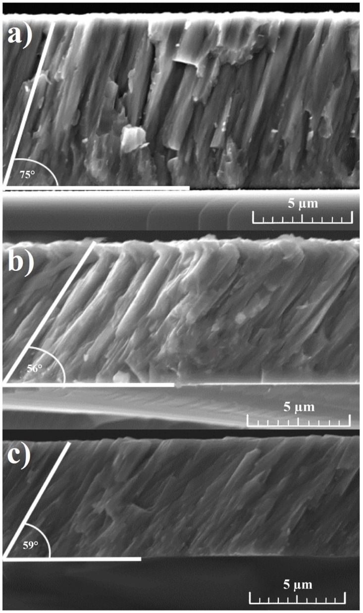
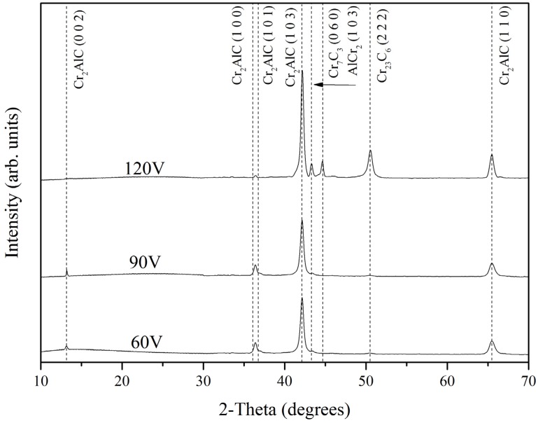
MAX phases (M = transition metal, A = A-group element, and X = C/N) are of special interest because they possess a unique combination of the advantages of both metals and ceramics. Most attention is attracted to the ternary carbide Cr2AlC because of its excellent high-temperature oxidation, as well as hot corrosion resistance. Despite lots of publications, up to now the influence of bias voltage on the chemical bonding structure, surface morphology, and mechanical properties of the film is still not well understood. In the current study, Cr-Al-C films were deposited on silicon wafers (100) and Inconel 718 super alloy by dc magnetron sputtering with different substrate bias voltages and investigated using Scanning Electron Microscopy (SEM), X-ray Photoelectron Spectroscopy (XPS), X-ray Diffraction (XRD), Atomic Force Microscopy (AFM), and nanoindentation. Transmission Electron Microscopy (TEM) was used to analyze the correlation between the growth of the films and the coating microstructure. The XPS results confirm the presence of Cr2AlC MAX phase due to a negative shift of 0.6-0.9 eV of the Al2p to pure aluminum carbide peak. The XRD results reveal the presence of Cr2AlC MAX Phase and carbide phases, as well as intermetallic AlCr2. The film thickness decreases from 8.95 to 6.98 µm with increasing bias voltage. The coatings deposited at 90 V exhibit the lowest roughness (33 nm) and granular size (76 nm) combined with the highest hardness (15.9 GPa). The ratio of Al carbide to carbide-like carbon state changes from 0.12 to 0.22 and correlates with the mechanical properties of the coatings. TEM confirms the columnar structure, with a nanocrystalline substructure, of the films.
Keywords: AFM; MAX phase; TEM; XPS; chemical bonding; surface morpholog.
Conflict of interest statement
The authors declare no conflict of interest.
Figures


References
-
- Barsoum M.W. The Mn + 1AXn phases: A new class of solids: Thermodynamically stable nanolaminates. Prog. Solid State Chem. 2000;28:201–281. doi: 10.1016/S0079-6786(00)00006-6. - DOI
-
- Jeitschko W., Nowotny H., Benesovsky F. Ti2AlN, eine stickstoffhaltige H-Phase. Monatshefte Chem. Verwandte Teile And. Wiss. 1963;94:1198–1200. doi: 10.1007/BF00905710. - DOI
-
- Jeitschko W., Nowotny H., Benesovsky F. Kohlenstoffhaltige ternäre Verbindungen (H-Phase) Monatshefte Chem. Verwandte Teile And. Wiss. 1963;94:672–676. doi: 10.1007/BF00913068. - DOI
-
- Lin Z., Zhou Y., Li M. Synthesis, Microstructure, and Property of Cr2AlC. J. Mater. Sci. Technol. 2007;23:721–746.
-
- Eklund P., Beckers M., Jansson U., Högberg H., Hultman L. The Mn + 1AXn phases: Materials science and thin-film processing. Thin Solid Films. 2010;518:1851–1878. doi: 10.1016/j.tsf.2009.07.184. - DOI
LinkOut - more resources
Full Text Sources
Other Literature Sources
Miscellaneous
