

Transparent Thin-Film Transistors Based on Sputtered Electric Double Layer
- PMID: 28772789
- PMCID: PMC5506904
- DOI: 10.3390/ma10040429
Transparent Thin-Film Transistors Based on Sputtered Electric Double Layer
Abstract
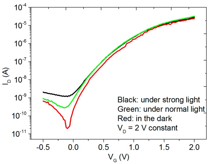
Electric-double-layer (EDL) thin-film transistors (TFTs) have attracted much attention due to their low operation voltages. Recently, EDL TFTs gated with radio frequency (RF) magnetron sputtered SiO₂ have been developed which is compatible to large-area electronics fabrication. In this work, fully transparent Indium-Gallium-Zinc-Oxide-based EDL TFTs on glass substrates have been fabricated at room temperature for the first time. A maximum transmittance of about 80% has been achieved in the visible light range. The transparent TFTs show a low operation voltage of 1.5 V due to the large EDL capacitance (0.3 µF/cm² at 20 Hz). The devices exhibit a good performance with a low subthreshold swing of 130 mV/dec and a high on-off ratio > 10⁵. Several tests have also been done to investigate the influences of light irradiation and bias stress. Our results suggest that such transistors might have potential applications in battery-powered transparent electron devices.
Keywords: electric-double-layer (EDL); radio frequency (RF) magnetron sputtered SiO2; transparent thin-film transistors (TFTs).
Conflict of interest statement
The authors declare no conflict of interest.
Figures


References
-
- Fortunato E., Correia N., Barquinha P., Pereira L., Gonçalves G., Martins R. High-performance flexible hybrid field-effect transistors based on cellulose fiber paper. IEEE Electron Device Lett. 2008;29:988–990. doi: 10.1109/LED.2008.2001549. - DOI
-
- Yabuta H., Sano M., Abe K., Aiba T., Den T., Kumomi H., Nomura K., Kamiya T., Hosono H. High-mobility thin-film transistor with amorphous InGaZnO4 channel fabricated by room temperature rf-magnetron sputtering. Appl. Phys. Lett. 2006;89:2123. doi: 10.1063/1.2353811. - DOI
-
- Hirao T., Furuta M., Hiramatsu T., Matsuda T., Li C., Furuta H., Hokari H., Yoshida M., Ishii H., Kakegawa M. Bottom-gate Zinc oxide thin-film transistors (ZnO TFTs) for AM-LCDs. IEEE Trans. Electron Devices. 2008;55:3136–3142. doi: 10.1109/TED.2008.2003330. - DOI
-
- Görrn P., Sander M., Meyer J., Kröger M., Becker E., Johannes H.H., Kowalsky W., Riedl T. Towards see-through displays: Fully transparent thin-film transistors driving transparent organic light-emitting diodes. Adv. Mater. 2006;18:738–741. doi: 10.1002/adma.200501957. - DOI
LinkOut - more resources
Full Text Sources
Other Literature Sources
Research Materials
