

Nanotwinned metal MEMS films with unprecedented strength and stability
- PMID: 28782015
- PMCID: PMC5489264
- DOI: 10.1126/sciadv.1700685
Nanotwinned metal MEMS films with unprecedented strength and stability
Abstract
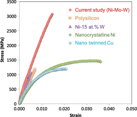
Silicon-based microelectromechanical systems (MEMS) sensors have become ubiquitous in consumer-based products, but realization of an interconnected network of MEMS devices that allows components to be remotely monitored and controlled, a concept often described as the "Internet of Things," will require a suite of MEMS materials and properties that are not currently available. We report on the synthesis of metallic nickel-molybdenum-tungsten films with direct current sputter deposition, which results in fully dense crystallographically textured films that are filled with nanotwins. These films exhibit linear elastic mechanical behavior and tensile strengths exceeding 3 GPa, which is unprecedented for materials that are compatible with wafer-level device fabrication processes. The ultrahigh strength is attributed to a combination of solid solution strengthening and the presence of dense nanotwins. These films also have excellent thermal and mechanical stability, high density, and electrical properties that are attractive for next-generation metal MEMS applications.
Keywords: Ni alloy; metal MEMS; nanotwins; thermal and mechanical stability; ultra high strength.
Figures
References
-
- S. E. Lyshevski, MEMS and NEMS: Systems, Devices, and Structures (CRC Press, 2002).
-
- C. T. Leondes, MEMS/NEMS Handbook Techniques and Applications (Springer, 2006).
-
- Krogstad J. A., Keimel C., Hemker K. J., Emerging materials for microelectromechanical systems at elevated temperatures. J. Mater. Res. 29, 1597–1608 (2014).
-
- Neudeck P. G., Okojie R. S., Chen L.-Y., High-temperature electronics—A role for wide bandgap semiconductors? Proc. IEEE 90, 1065–1076 (2002).
-
- Liew L. A., Zhang W. G., An L. N., Shah S., Luo R. L., Liu Y. P., Cross T., Dunn M. L., Bright V., Daily J. W., Raj R., Anseth K., Ceramic MEMS—New materials, innovative processing and future applications. Am. Ceram. Soc. Bull. 80, 25–30 (2001).
Publication types
LinkOut - more resources
Full Text Sources
Other Literature Sources
