

Mechanical Properties of Cu₂O Thin Films by Nanoindentation
- PMID: 28788343
- PMCID: PMC5452851
- DOI: 10.3390/ma6104505
Mechanical Properties of Cu₂O Thin Films by Nanoindentation
Abstract
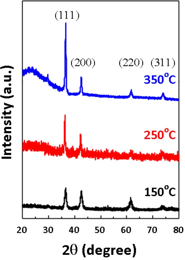
In this study, the structural and nanomechanical properties of Cu₂O thin films are investigated by X-ray diffraction (XRD), atomic force microscopy (AFM), scanning electron microscopy (SEM) and nanoindentation techniques. The Cu₂O thin films are deposited on the glass substrates with the various growth temperatures of 150, 250 and 350 °C by using radio frequency magnetron sputtering. The XRD results show that Cu₂O thin films are predominant (111)-oriented, indicating a well ordered microstructure. In addition, the hardness and Young's modulus of Cu₂O thin films are measured by using a Berkovich nanoindenter operated with the continuous contact stiffness measurements (CSM) option. Results indicated that the hardness and Young's modulus of Cu₂O thin films decreased as the growth temperature increased from 150 to 350 °C. Furthermore, the relationship between the hardness and films grain size appears to closely follow the Hall-Petch equation.
Keywords: AFM; Cu2O thin film; SEM; XRD; hardness; nanoindentation.
Conflict of interest statement
The authors declare that they no conflict of interest.
Figures


References
-
- Akimoto K., Ishizuka S., Yanagita M., Nawa Y., Paul G.K., Sakurai T. Thin film deposition of Cu2O and application for solar cells. Sol. Energy. 2006;80:715–722. doi: 10.1016/j.solener.2005.10.012. - DOI
-
- Hussain S., Cao C.B., Usman Z., Chen Z., Nabi G., Khan W.S., Ali Z., Butt F.K., Mahmood T. Fabrication and photovoltaic characteristics of Cu2O/TiO2 thin film heterojunction solar cell. Thin Solid Films. 2012;522:430–434. doi: 10.1016/j.tsf.2012.08.013. - DOI
-
- Minami T., Nishi Y., Miyata T. High-efficiency Cu2O-based heterojunction solar cells fabricated using a Ga2O3 thin film as N-type layer. Appl. Phys. Express. 2013;6:044101:1–044101:4. doi: 10.7567/APEX.6.044101. - DOI
-
- Ristov M., Sinadinovski G., Mitreski M. Chemically deposited Cu2O thin-film as an oxygen-pressure sensor. Thin Solid Films. 1988;167:309–316. doi: 10.1016/0040-6090(88)90508-1. - DOI
-
- Jian S.R., Juang J.Y. Nanoindentation-induced pop-in effects in GaN thin films. IEEE Trans. Nanotech. 2013;12:304–308. doi: 10.1109/TNANO.2013.2240313. - DOI
LinkOut - more resources
Full Text Sources
Other Literature Sources
Miscellaneous
