

Fabrication of X-ray Microcalorimeter Focal Planes Composed of Two Distinct Pixel Types
- PMID: 28804229
- PMCID: PMC5548520
- DOI: 10.1109/TASC.2016.2633783
Fabrication of X-ray Microcalorimeter Focal Planes Composed of Two Distinct Pixel Types
Abstract
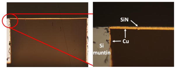
We are developing superconducting transition-edge sensor (TES) microcalorimeter focal planes for versatility in meeting specifications of X-ray imaging spectrometers including high count-rate, high energy resolution, and large field-of-view. In particular, a focal plane composed of two sub-arrays: one of fine-pitch, high count-rate devices and the other of slower, larger pixels with similar energy resolution, offers promise for the next generation of astrophysics instruments, such as the X-ray Integral Field Unit (X-IFU) instrument on the European Space Agency's Athena mission. We have based the sub-arrays of our current design on successful pixel designs that have been demonstrated separately. Pixels with an all gold X-ray absorber on 50 and 75 micron scales where the Mo/Au TES sits atop a thick metal heatsinking layer have shown high resolution and can accommodate high count-rates. The demonstrated larger pixels use a silicon nitride membrane for thermal isolation, thinner Au and an added bismuth layer in a 250 micron square absorber. To tune the parameters of each sub-array requires merging the fabrication processes of the two detector types. We present the fabrication process for dual production of different X-ray absorbers on the same substrate, thick Au on the small pixels and thinner Au with a Bi capping layer on the larger pixels to tune their heat capacities. The process requires multiple electroplating and etching steps, but the absorbers are defined in a single ion milling step. We demonstrate methods for integrating heatsinking of the two types of pixel into the same focal plane consistent with the requirements for each sub-array, including the limiting of thermal crosstalk. We also discuss fabrication process modifications for tuning the intrinsic transition temperature (Tc) of the bilayers for the different device types through variation of the bilayer thicknesses. The latest results on these "hybrid" arrays will be presented.
Keywords: Arrays; X-ray spectroscopy; low temperature detectors; microcalorimeters; transition-edge sensors (TES).
Figures


References
-
- Barcons X, Nandra K, Barret D, den Herder J-W, Fabian AC, Piro L, Watson MG the Athena team. Athena: the X-ray Observatory to study the hot and energetic universe. J of Physics Conference Series. 2015 May;610:012008.
-
- Barret D, Lam Trong T, den Herder J-W, Piro L, Barcons X the Athena team. The Athena X-ray Integral Field Unit. Proc SPIE 9905, Space Telescopes and Instrumentation 2016: Ultraviolet to Gamma Ray. 2016 Aug;:99052F.
-
- Smith SJ, et al. Transition edge sensor pixel parameter design of the microcalorimeter array for the X-ray Integral Field Unit on Athena. Proc SPIE. 2016;9905:99052H.
-
- Sadleir JE, Smith SJ, Bandler SR, Chervenak JA, Clem JR. Longitudinal Proximity Effects in Superconducting Transition-Edge Sensors. Phys Rev Lett. 2010 Jan;104(4) - PubMed
-
- Smith SJ, Adams JS, Bailey CN, Bandler SR, Chervenak JA, Eckart ME, Finkbeiner FM, Kelley RL, Kilbourne CA, Porter FS, Sadleir JE. Small pitch transition-edge sensors with broadband high spectral resolution for solar physics. J Low Temp Phys. 2012 Feb;167:168–175.
Grants and funding
LinkOut - more resources
Full Text Sources
Other Literature Sources