

Maskless X-Ray Writing of Electrical Devices on a Superconducting Oxide with Nanometer Resolution and Online Process Monitoring
- PMID: 28831111
- PMCID: PMC5567384
- DOI: 10.1038/s41598-017-09443-3
Maskless X-Ray Writing of Electrical Devices on a Superconducting Oxide with Nanometer Resolution and Online Process Monitoring
Abstract
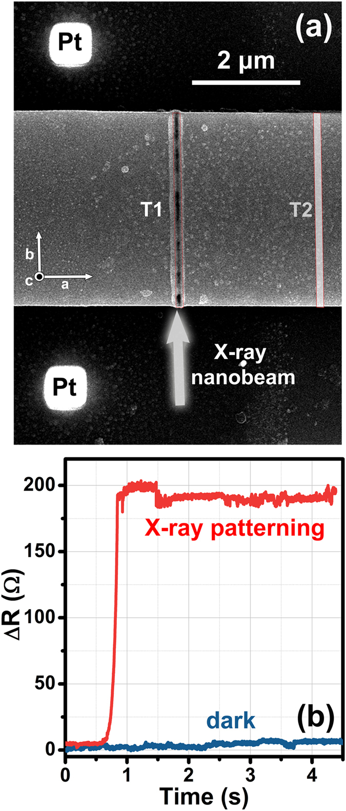
X-ray nanofabrication has so far been usually limited to mask methods involving photoresist impression and subsequent etching. Herein we show that an innovative maskless X-ray nanopatterning approach allows writing electrical devices with nanometer feature size. In particular we fabricated a Josephson device on a Bi2Sr2CaCu2O8+δ (Bi-2212) superconducting oxide micro-crystal by drawing two single lines of only 50 nm in width using a 17.4 keV synchrotron nano-beam. A precise control of the fabrication process was achieved by monitoring in situ the variations of the device electrical resistance during X-ray irradiation, thus finely tuning the irradiation time to drive the material into a non-superconducting state only in the irradiated regions, without significantly perturbing the crystal structure. Time-dependent finite element model simulations show that a possible microscopic origin of this effect can be related to the instantaneous temperature increase induced by the intense synchrotron picosecond X-ray pulses. These results prove that a conceptually new patterning method for oxide electrical devices, based on the local change of electrical properties, is actually possible with potential advantages in terms of heat dissipation, chemical contamination, miniaturization and high aspect ratio of the devices.
Conflict of interest statement
The authors declare that they have no competing interests.
Figures


References
-
- Seisyan RP. Nanolithography in microelectronics: A review. Tech. Phys. 2011;56:1061–1073. doi: 10.1134/S1063784211080214. - DOI
-
- Romanato F, et al. Fabrication of 3D metallic photonic crystals by X-ray lithography. Microelectron. Eng. 2003;67-8:479–486. doi: 10.1016/S0167-9317(03)00104-7. - DOI
-
- Maldonado JR, Peckerar M. X-ray lithography: Some history, current status and future prospects. Microelectron. Eng. 2016;161:87–93. doi: 10.1016/j.mee.2016.03.052. - DOI
-
- Cerrina F. X-ray imaging: applications to patterning and lithography. J. Phys. D-Appl. Phys. 2000;33:R103–R116. doi: 10.1088/0022-3727/33/12/201. - DOI
Publication types
LinkOut - more resources
Full Text Sources
Other Literature Sources
Research Materials
