Review
. 2017 Aug 25;17(9):1962.
doi: 10.3390/s17091962.

Review of CMOS Integrated Circuit Technologies for High-Speed Photo-Detection

Affiliations
Review

Review of CMOS Integrated Circuit Technologies for High-Speed Photo-Detection

Gyu-Seob Jeong et al. Sensors (Basel). .

Abstract

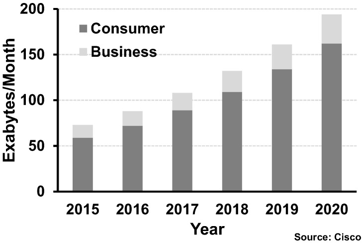
The bandwidth requirement of wireline communications has increased exponentially because of the ever-increasing demand for data centers and high-performance computing systems. However, it becomes difficult to satisfy the requirement with legacy electrical links which suffer from frequency-dependent losses due to skin effects, dielectric losses, channel reflections, and crosstalk, resulting in a severe bandwidth limitation. In order to overcome this challenge, it is necessary to introduce optical communication technology, which has been mainly used for long-reach communications, such as long-haul networks and metropolitan area networks, to the medium- and short-reach communication systems. However, there still remain important issues to be resolved to facilitate the adoption of the optical technologies. The most critical challenges are the energy efficiency and the cost competitiveness as compared to the legacy copper-based electrical communications. One possible solution is silicon photonics which has long been investigated by a number of research groups. Despite inherent incompatibility of silicon with the photonic world, silicon photonics is promising and is the only solution that can leverage the mature complementary metal-oxide-semiconductor (CMOS) technologies. Silicon photonics can be utilized in not only wireline communications but also countless sensor applications. This paper introduces a brief review of silicon photonics first and subsequently describes the history, overview, and categorization of the CMOS IC technology for high-speed photo-detection without enumerating the complex circuital expressions and terminologies.

Keywords: CMOS; integrated circuit; photodetector; silicon photonics; transimpedance amplifier.


Conflict of interest statement

The authors declare no conflict of interest.

Figures

Figure 1
Figure 1
Forecast of total global IP traffic [1].
Figure 2
Figure 2
Forecast of global IP traffic (a) by application and (b) by video content [1].
Figure 3
Figure 3
(a) Power breakdown of data centers and (b) forecast of IP traffic contribution [1].
Figure 4
Figure 4
Trends of copper-based electrical links from recent 10-year ISSCC papers.
Figure 5
Figure 5
Summary of communication standards, Ethernet.
Figure 6
Figure 6
2 × 10-Gb/s dual channel optoelectronic transceiver [44].
Figure 7
Figure 7
Monolithic receiver with PD splitting [46].
Figure 8
Figure 8
Block diagram of memory-processor optical link realized in [48].
Figure 9
Figure 9
Cross-section of photonic and electronic devices [49].
Figure 10
Figure 10
Monolithically integrated DWDM optical link in bulk CMOS [50].
Figure 11
Figure 11
Schematic view of EPIC structure [51].
Figure 12
Figure 12
Block diagram of optical transceiver [51].
Figure 13
Figure 13
Illustration of wire-bonded EIC and PIC.
Figure 14
Figure 14
Illustration of flip-chip package [54].
Figure 15
Figure 15
Implementation of 2-D array of EPIC [55].
Figure 16
Figure 16
Flip-chip bonded EIC directly on PIC using micro bump [56].
Figure 17
Figure 17
EIC flip-chip bonded to macro-PIC [43].
Figure 18
Figure 18
Cross-sectional view of waveguide PD [58].
Figure 19
Figure 19
Schematic view of silicon resonator-enhanced PD [60].
Figure 20
Figure 20
Categorization of PD by coupling schemes.
Figure 21
Figure 21
Simple implementation of TIA using single resistor.
Figure 22
Figure 22
Common-gate TIA.
Figure 23
Figure 23
Regulated-cascode TIA.
Figure 24
Figure 24
CG-feedforward TIA.
Figure 25
Figure 25
Shunt-shunt feedback TIA.
Figure 26
Figure 26
Various implementations of shunt-shunt feedback TIA. (a) CS amplifier with resistor feedback, (b) Cascaded CS amplifier and source follower with resistor feedback, and (c) multi-stage amplifier with resistor feedback.
Figure 27
Figure 27
Inverter-based TIA.
Figure 28
Figure 28
Integrating receiver based on double sampling.
Figure 29
Figure 29
Circuit diagrams of (a) CS stage without inductive peaking, (b) CS stage with shunt peaking, (c) and CS stage with series peaking.
Figure 30
Figure 30
Circuit diagrams of (a) shunt and series peaking, (b) shunt and double-series peaking, (c) and T-coil peaking network.
Figure 31
Figure 31
TIA with shunt peaking presented in [80].
Figure 32
Figure 32
Three-stage TIA with series peaking presented in [65].
Figure 33
Figure 33
TIA examples with series peaking between cascaded gain stages presented in (a) [61] and (b) [71].
Figure 34
Figure 34
CG TIA with T-coil peaking presented in [82].
Figure 35
Figure 35
Effect of feedback on the transfer function of an amplifier (a) with only resistive feedback (b) with the combination of resistive and inductive feedback.
Figure 36
Figure 36
(a) Miller effect (b) Miller capacitance applied in a differential CS stage in [91].
Figure 37
Figure 37
Summary of CTLE based on source degenerated CS stage. (ac) Circuit diagrams of normal CS stage, CS stage with source degeneration resistor, and CS stage with source degeneration resistor and capacitor (CTLE). (d) Transfer function of CTLE.
Figure 38
Figure 38
Overall structure of [91].
Figure 39
Figure 39
Simplified block diagram of DFE.
Figure 40
Figure 40
Resistor-based TIA with IIR-DFE proposed in [55].
Figure 41
Figure 41
Dependency of BER on sampling timing. (a) Qualitative explanation of BER degradation and (b) quantitative relation of BER with sampling timing using the formula in [105].
Figure 42
Figure 42
Simplified block diagram of a complete high-speed photodetecting receiver including CDR.
Figure 43
Figure 43
Sequential locking CDR presented in [29].
Figure 44
Figure 44
Dual loop CDR with integration-based front-end presented in [78].
Figure 45
Figure 45
All-digital CDR presented in [74].

References

    1. Cisco Systems, Inc. [(accessed on 19 June 2017)]; Available online: http://www.cisco.com.
    1. Soref R.A. Silicon-based optoelectronics. Proc. IEEE. 1993;81:1687–1706. doi: 10.1109/5.248958. - DOI
    1. Izhaky N., Morse M.T., Koehl S., Cohen O., Rubin D., Barkai A., Sarid G., Cohen R., Paniccia M.J. Development of CMOS-compatible integrated silicon photonics devices. IEEE J. Sel. Top. Quantum Electron. 2006;12:1688–1698. doi: 10.1109/JSTQE.2006.884089. - DOI
    1. Vlasov Y.A. Silicon CMOS-integrated nano-photonics for computer and data communications beyond 100G. IEEE Commun. Mag. 2012;50:s67–s72. doi: 10.1109/MCOM.2012.6146487. - DOI
    1. Fedeli J.-M., Fulbert L., Van Thourhout D., Viktorovitch P., O’Connor I., Duan G.-H., Reed G., Corte F.D., Vivien L., Royo F.L., et al. HELIOS: Photonics electronics functional integration on CMOS. SPIE Proc. 2010;7719:1–10.