Review
. 2017 Feb 16;4(8):1600430.
doi: 10.1002/advs.201600430. eCollection 2017 Aug.

Plasmonics of 2D Nanomaterials: Properties and Applications

Affiliations
Review

Plasmonics of 2D Nanomaterials: Properties and Applications

Yu Li et al. Adv Sci (Weinh). .

Abstract

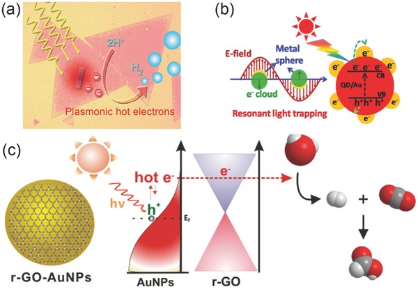
Plasmonics has developed for decades in the field of condensed matter physics and optics. Based on the classical Maxwell theory, collective excitations exhibit profound light-matter interaction properties beyond classical physics in lots of material systems. With the development of nanofabrication and characterization technology, ultra-thin two-dimensional (2D) nanomaterials attract tremendous interest and show exceptional plasmonic properties. Here, we elaborate the advanced optical properties of 2D materials especially graphene and monolayer molybdenum disulfide (MoS2), review the plasmonic properties of graphene, and discuss the coupling effect in hybrid 2D nanomaterials. Then, the plasmonic tuning methods of 2D nanomaterials are presented from theoretical models to experimental investigations. Furthermore, we reveal the potential applications in photocatalysis, photovoltaics and photodetections, based on the development of 2D nanomaterials, we make a prospect for the future theoretical physics and practical applications.

Keywords: 2D materials; light‐matter interactions; optoelectronics; surface plasmons.


Figures

Figure 1
Figure 1
a) Schematic view of the light absorption process in graphene: excitation, relaxation and absorption block. Reproduced with permission.[30] b) Optical image of graphene and its bilayer. (Inset) the experimental sample design. Reproduced with permission.[8] Copyright 2008, AAAS. c) Schematics of A, B exciton and A− trion formation in MoS2 monolayer. Reproduced with permission.[37] Copyright 2014, ACS. d) Electroluminescence mapping of monolayer MoS2. Reproduced with permission.[43] Copyright 2013, ACS. e) PL spectrum. (Inset) the schematic view of MoS2 monolayer comprising trion and exciton component. Reproduced with permission.[37] Copyright 2014, ACS. f) Comparing absorption (Abs), EL, and PL spectra of monolayer MoS2. Reproduced with permission.[43] Copyright 2013, ACS.
Figure 2
Figure 2
a) Optical conductivities of pristine monolayer and bilayer graphene, doped monolayer and bilayer graphene and fluorographene. (Inset) enlarged spectral in the low energy region. Reproduced with permission.[52] Copyright 2012, Nature Publishing Group. b) Plasmonic propagation length and SPP wavelength of graphene and gold. Reproduced with permission.[53] Copyright 2012, Nature Publishing Group. c) Surface plasmon loss spectrum of graphene in different momentum transfer condition. d) Plasmon dispersion of graphene and free 2D electron gas at the same electron density. (Inset) the band structure of graphene. c,d) Reproduced with permission.[14] Copyright 2008, APS. e) Angle‐resolved photoemission spectra of doped graphene on SiC and schematic view of interacting and non‐interacting Dirac energy spectra. Reproduced with permission.[63] Copyright 2010, AAAS.
Figure 3
Figure 3
a) SEM image of MoS2/silver nanodisk hybrid structure on a Si/SiO2 substrate. b) Angle‐resolved differential reflectance spectra of MoS2/silver nanodisk hybrid structure, solid lines are multi‐oscillators model fitted results. (a,b) Reproduced with permission.[79] Copyright 2016, ACS. c) Peak transmission energies as a function of in‐plane angular momentum for MoS2/FP cavity hybrid structure, the Rabi splitting of 101meV exist between P+ and P‐ branch. (Inset) the schematic view of the hybrid structure. d) Photoluminescence dispersion of MoS2/plasmonic hole array hybrid structure. (Inset) the schematic view of the hybrid structure.(c,d) Reproduced with permission.[27] Copyright 2016, ACS.
Figure 4
Figure 4
a) Plasmonic response of graphene with different carrier density. b) Graphene IR reflection spectra with various sheet carrier density. a,b) Reproduced with permission.[80] Copyright 2015, De Gruyter. c) Plasmon dispersion relation in doped graphene. (Inset) the propagation decay in the unit of SPP wavelength. Reproduced with permission.[81] Copyright 2011, ACS. d) Left panel shows PL images of monolayer drop‐casted MoS2, the right shows the absorption spectrum of 2D nanoflakes under electrochemical force control. e) Schematics of plasmon resonance peak positions as the function of Li+ ions number in 2D MoS2 nanoflakes for 2H and 1T phases. d,e) Reproduced with permission.[82] Copyright 2015, ACS.
Figure 5
Figure 5
a) Near‐field images of resonant localized mode on tapered graphene ribbon taken with different imaging wavelength. Reproduced with permission.[86] Copyright 2012, Nature Publishing Group. b) Photograph of graphene in IR spectrum region, the wave pattern shows significant boundary and defect sensitivity. Reproduced with permission.[87] Copyright 2012, Nature Publishing Group. c) Left: structure of graphene disks array device, right: corresponding transition and reflection spectra with changing disk diameter. Reproduced with permission.[89] Copyright 2014, ACS. d) Left: AFM image of different widths of graphene ribbon arrays, right: Localized plasmonic resonance induced extinction spectral in monolayer graphene ribbons. Reproduced with permission.[91] Copyright 2011, Nature Publishing Group. e) Experiment and simulation results of localized plasmonic resonance modes analysis in graphene disks on SiO2 substrate. Reproduced with permission.[90] Copyright 2016, Nature Publishing Group. f) Upper: graphene ribbon pairs, lower: near field image of two plasmonic resonance mode. Reproduced with permission.[92] Copyright 2011, ACS.
Figure 6
Figure 6
a) Top: illustration of graphene‐gold nanorod hybrid structure, bottom: Rayleigh scattering spectra of hybrid structure at different gate voltage. (Inset) SEM image of nanorod on graphene sample. Reproduced with permission.[103] Copyright 2012, ACS. b) Top: schematic illustration of electrically tunable graphene‐bowtie antennas hybrid structure, middle: changes of plasmonic resonance damping under applied gate voltage, bottom: plasmonic resonance width changing as the function of gate voltage. Reproduced with permission.[104] Copyright 2012, ACS. c) Upper: illustration of graphene ribbon array hybridized with metal gratings structure, lower: absorption mapping of the structure with changing trench width. Reproduced with permission.[101] Copyright 2015, ACS. d) The spectral position of the A exciton and two polariton branches for both pristine MoS2 and nanodisk‐MoS2 hybrid structure as the function of temperature. Reproduced with permission.[79] Copyright 2016, ACS. e) Upper: schematic view of Fano‐resonant structure hybrid gated graphene structure, lower: the reflectance spectrum under electrical switching. Reproduced with permission.[99] Copyright 2015, ACS. f) Upper: illustration of Ag disk‐MoS2 hybrid structure under laser illumination, lower: changing of localized plasmon shifting as the laser power changes. Reproduced with permission.[96]
Figure 7
Figure 7
a) Upper: graphene quantum dots and monolayer MoS2 heterostructure and the charge transfer illustration, bottom: PL spectrum of MoS2 changes with the GQDs concentration. Reproduced with permission.[113] b) Upper: sketch, SEM image and PL mapping of Ag‐MoS2 hybrid structure, bottom: PL spectrum intensity is influenced by Ag disks modification as well as the diameter of nanodisk. (Inset) cross‐section view of the sample design. Reproduced with permission.[117] Copyright 2015, ACS. c) Upper: PL spectrum of 5nm diameter Au NPs deposited MoS2 and pristine 2D MoS2 sheet, lower: characteristic Raman spectrum of Au‐MoS2 hybrid structure. Reproduced with permission.[118] d) Upper: PL spectra of MoS2 on SiO2/Si substrate, MoS2 on gold nanoantenna and bare gold nanoantenna, lower: corresponding PL intensity mapping. Reproduced with permission.[119] Copyright 2014, ACS. e): Upper: schematics of launching and propagation of SPPs coupled with excitons, bottom left: optical image of the hybrid structure illuminated by laser, bottom right: PL spectral of MoS2 samples with and without nanowires. (Inset): cross‐section of structure design. Reproduced with permission.[121] Copyright 2015, APS. f) Upper: SEM images of four types of Ag NPs, lower: schematics of Ag NPs modified PL measuring method. Reproduced with permission.[123]
Figure 8
Figure 8
a) Illustration of graphene photodetector with gate bias. Reproduced with permission.[127] Copyright 2012, Nature Publishing Group. b) Upper: schematic view of monolayer MoS2 based photodetector, bottom: gating response in dark/illuminated state. Reproduced with permission.[129] Copyright 2013, Nature Publishing Group. c) Plasmonic structures coupled bilayer MoS2 photodetection. Reproduced with permission.[130] Copyright 2015, ACS. d) Upper: illustration of nanoantennas sandwiched graphene photodetector, bottom: PL spectral as the function of line scan position. (Inset) polarization dependent photocurrent response. Reproduced with permission.[131] Copyright 2012, ACS. e) Two kinds of plasmonic nanostructure enhanced graphene photodetectors. f) Surface plasmon polaritons coupled graphene photodetector. (e,f) Reproduced with permission.[134] Copyright 2015, ACS.
Figure 9
Figure 9
a) Schematic view of single layer MoS2 catalysis in hydrogen evolution reaction supported by plasmonic hot electron. Reproduced with permission.[20] Copyright 2015, RSC. b) The illustration of localized SPR effect induced charge separation and transfer process in heteronanocrystals supported by graphene. Reproduced with permission.[19] Copyright 2014, ACS. c) Graphene‐coated gold nanoparticles and the schematics showing photoconversion mechanism of CO2 into HCOOH. Reproduced with permission.[143] Copyright 2016, ACS.

References

    1. Mak K. F., Lee C., Hone J., Shan J., Heinz T. F., Phys. Rev. Lett. 2010, 105, 136805. - PubMed
    1. Dai S., Fei Z., Ma Q., Rodin A. S., Wagner M., McLeod A. S., Liu M. K., Gannett W., Regan W., Watanabe K., Science 2014, 343, 1125. - PubMed
    1. Lin Y., Williams T. V., Connell J. W., J. Phys. Chem. Lett. 2009, 1, 277.
    1. Radisavljevic B., Radenovic A., Brivio J., Giacometti V., Kis A., Nat. Nanotechnol. 2011, 6, 147. - PubMed
    1. Geim A. K., Novoselov K. S., Nat. Mater. 2007, 6, 183. - PubMed