. 2017 Sep 7;7(1):10850.
doi: 10.1038/s41598-017-10534-4.

Graphene Quantum Dot Solid Sheets: Strong blue-light-emitting & photocurrent-producing band-gap-opened nanostructures

Affiliations

Graphene Quantum Dot Solid Sheets: Strong blue-light-emitting & photocurrent-producing band-gap-opened nanostructures

Ganapathi Bharathi et al. Sci Rep. .

Abstract

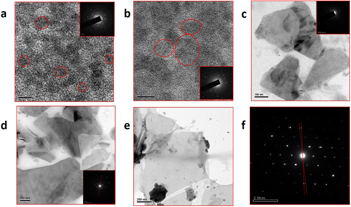
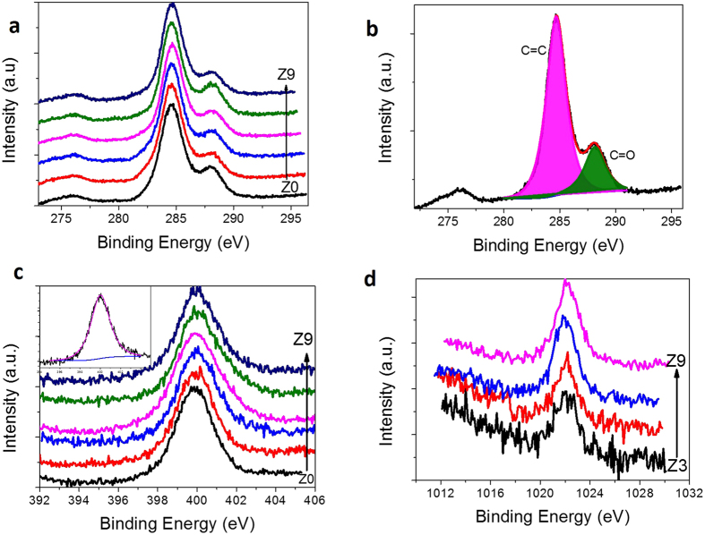
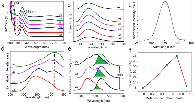
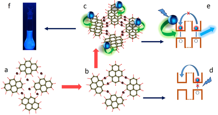
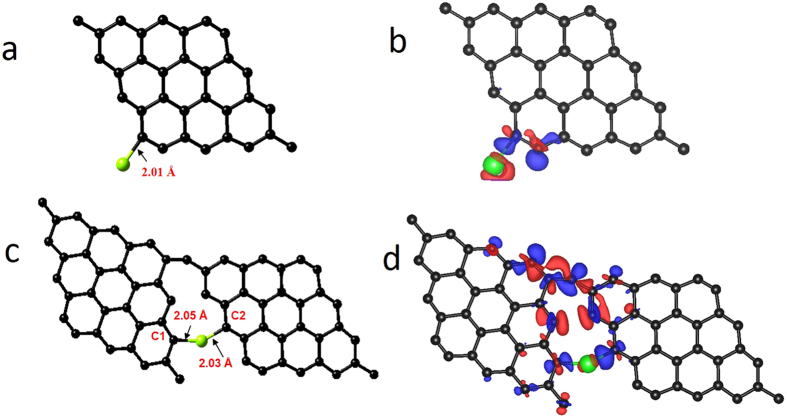
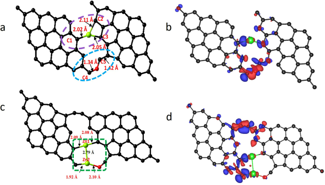
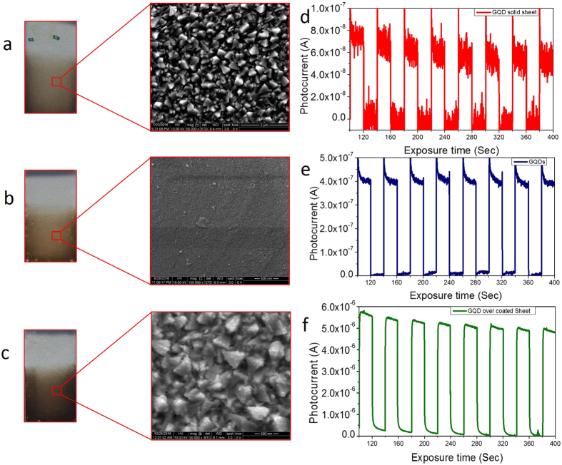
Graphene has been studied intensively in opto-electronics, and its transport properties are well established. However, efforts to induce intrinsic optical properties are still in progress. Herein, we report the production of micron-sized sheets by interconnecting graphene quantum dots (GQDs), which are termed 'GQD solid sheets', with intrinsic absorption and emission properties. Since a GQD solid sheet is an interconnected QD system, it possesses the optical properties of GQDs. Metal atoms that interconnect the GQDs in the bottom-up hydrothermal growth process, induce the semiconducting behaviour in the GQD solid sheets. X-ray absorption measurements and quantum chemical calculations provide clear evidence for the metal-mediated growth process. The as-grown graphene quantum dot solids undergo a Forster Resonance Energy Transfer (FRET) interaction with GQDs to exhibit an unconventional 36% photoluminescence (PL) quantum yield in the blue region at 440 nm. A high-magnitude photocurrent was also induced in graphene quantum dot solid sheets by the energy transfer process.


Conflict of interest statement

The authors declare that they have no competing interests.

Figures

Figure 1
Figure 1
HRTEM analysis of GQDs and GQD solid sheet structures. (a) Spherical shaped GQDs with size around 5 nm from Z0 sample (b) spherical shaped GQDs with size around 10 nm from the Z1 sample (c) slab like GQD solid sheets in 100 nm size range from Z3 sample (d–e) slab like GQD solid sheets having average size about 1µm from Z5 and Z7 samples, respectively. The samples Z0, Z1 and Z3 are polycrystalline in nature, as revealed by the SAED pattern given as the inset of respective figures. The Z5 and Z7 samples are single crystalline in nature. (f) An example SAED pattern obtained from the Z7 sample. The double diffraction spots represented by the red line, in the single crystalline SAED pattern reveals the presence of twinning effect in the solid sheet samples.
Figure 2
Figure 2
XPS analysis of GQDs and GQD solid sheet structures. (a) High resolution C1s spectra of GQDs and different sized solid sheets (Z0-Z9), (b) the deconvoluted C1s spectra as a representation, gives the evidence of graphitic C=C (at 284.6 eV) with less amount of carboxyl functionalities (at 288.1 eV), (c) N1s high resolution spectra showing the broad symmetric peak at 399.9 eV. It indicates that, the major contribution is from the graphitic nitrogen component. The inset shows the deconvoluted N1s spectra. (d) Zn2p high resolution spectra demonstrating the increase of Zn presence in the GQD solid sheets with increase in sheet size. XPS survey spectra and O1s spectra of all the as prepared samples are given in the Supplementary Fig. S2.
Figure 3
Figure 3
Optical properties of GQDs and GQD solid sheet structures. (a) UV-Vis absorption spectra of Z0-Z9 raw samples. It shows two absorption bands at 234 and 334 nm correspond to the π-π* (C=C) and n-π* (C=O/C=N) transitions, respectively, (b) emission spectra of raw samples showing increase in emission intensity upto Z7 and further a decrease for Z9 sample, (c) excitaion spectra of raw samples showing peak maxima at 350 nm, (d) excitation spectra of separated solid sheets show the shift in peak maxima from 350 to 410 nm for samples prepared with higher metal concentration, (e) spectral overlap between excitation of solid sheet samples [Z3, Z5 & Z7] and emission of GQD samples (f) A graph representing the quantum yield values as function of metal concentration in our samples. The excitation, emission, and quantum yield values are given as comparative table in the Supplementary Table S1.
Figure 4
Figure 4
Schematic representation of the proposed growth process. (a,b) Graphene quantum dots (GQDs) are interconnected through binding with metal atoms, (c) stacking of interconnected graphene solid sheet layers and indirect FRET excitation by the GQDs emission, (d) quantum well design of the sheet sample, representing the non radiative relaxation of photoexcited electrons, when excited directly. This is due to the delocalization of photoexcited e-h pairs. (e) In the solid sheet - GQDs coupled structure, the photoexcited electrons present in all the excited states because of the simultaneous excitation of all the domains by FRET process and therefore the delocalization process is suppressed, (f) Photographic image of Z7 sample when illuminated with UV light. The CIE chromaticity diagram representing the emission from Z7 sample is given in the Supplementary Fig. S8.
Figure 5
Figure 5
Raman analysis of GQDs and GQD solid sheet structures. (a) Raman spectra of the raw samples (Z0-Z7), showing D and G bands. The D band increases with the increase of metal concentration. (b) Optical microscope image of a GQD interconnected solid sheet (Z7), (c) Raman mapping of D band, (d) Raman mapping of G band, (e) area ratio of D band to G band. It clearly shows the distribution G and D bands in whole area of the solid sheet.
Figure 6
Figure 6
X-Ray absorption spectroscopy measurements of GQD solid sheet samples at Zn K-edge. (a) EXAFS spectra at Zn K-edge of solid sheet samples, (b) experimental χ(R) vs R data fitted with the theoretically generated plot at Zn k-edge, (c) enlarged absorption edge [near edge] of Zn K-edge spectra showing the higher valence state of Zn in our samples compared to that of metallic Zn, (d) normalized k 2 weighted χ(k) spectra of the GQD solid sheets at the Zn k-edge.
Figure 7
Figure 7
X-Ray absorption spectroscopy measurements of GQDs and GQD solid sheet structures at C, N and O K-edges. (a) C K-edge spectra of GQDs and solid sheet samples (Z0-Z9), (b) enlarged C-K edge spectra showing the rise of excitonic peak at 286.3 eV with metal doping effect, (c) N K-edge showing the presence of graphitic nitrogen with a sharp peak at 401.1 eV, (d) O K-edge spectra showing the presence of C-O and C=O in our samples.
Figure 8
Figure 8
Metal atom incorporated Graphene structure models used for DFT and Bader charge calculations. (a) Graphene sheet interacting with Zn atom at the edge site, (b) electron density difference plot of Zn-edge interacting graphene sheet, (c) graphene sheets interconnected through zinc atom, (d) electron density difference plots of graphene sheets interconnected with zinc atom. It provides the theoretical evidence for the interconnection process and the electron density difference plots show the sharing of charges in the interconnection process.
Figure 9
Figure 9
Metal and oxygen atoms incorporated Graphene structure models used for DFT and Bader charge calculations. (a) Graphene sheets interconnected through zinc and oxygen atoms with oxygen atom in the next to nearest neighbor position to Zn atom. The electron transfer region is highlighted with violet and blue circles. (b) Electron density difference plot of structure given in (a), (c) graphene sheets interconnected with two zinc atoms with oxygen atom in the nearest neighbor position. The electron transfer region is highlighted with green rectangle. (d) The electron density difference plot of structure given in (c).
Figure 10
Figure 10
FESEM images and photocurrent curves of EPD coated GQDs and GQD solid sheet structures. The photographic and FESEM images of, (a) GQD interconnected solid sheets, (b) graphene quantum dots (GQDs), (c) GQDs decorated on solid sheets, (df) corresponding photocurrent curves of (a,b and c). The photocurrent measurements show an abrupt raise in the photocurrent upon GQD decoration on solid sheets.

References

    1. Geim AK, Novoselov KS. The rise of graphene. Nat Mater. 2007;6:183–191. doi: 10.1038/nmat1849. - DOI - PubMed
    1. Kim TY, Park C-H, Marzari N. The Electronic Thermal Conductivity of Graphene. Nano Letters. 2016;16:2439–2443. doi: 10.1021/acs.nanolett.5b05288. - DOI - PubMed
    1. Griep MH, Sandoz-Rosado E, Tumlin TM, Wetzel E. Enhanced Graphene Mechanical Properties through Ultrasmooth Copper Growth Substrates. Nano Letters. 2016;16:1657–1662. doi: 10.1021/acs.nanolett.5b04531. - DOI - PubMed
    1. Novoselov KS. Graphene: The Magic of Flat Carbon. ECS Transactions. 2009;19:3–7. doi: 10.1149/1.3119522. - DOI
    1. Meija R, et al. Nanomechanics of individual aerographite tetrapods. 2017;8:14982. - PMC - PubMed

Publication types