Review
. 2017 Jul 28:8:1532-1545.
doi: 10.3762/bjnano.8.155. eCollection 2017.

Parylene C as a versatile dielectric material for organic field-effect transistors

Affiliations
Review

Parylene C as a versatile dielectric material for organic field-effect transistors

Tomasz Marszalek et al. Beilstein J Nanotechnol. .

Abstract

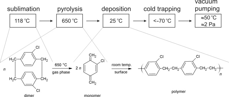
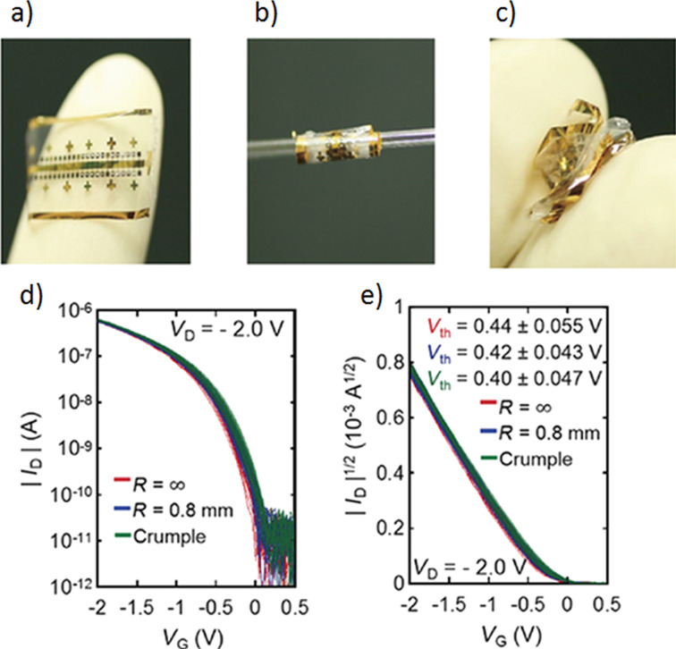
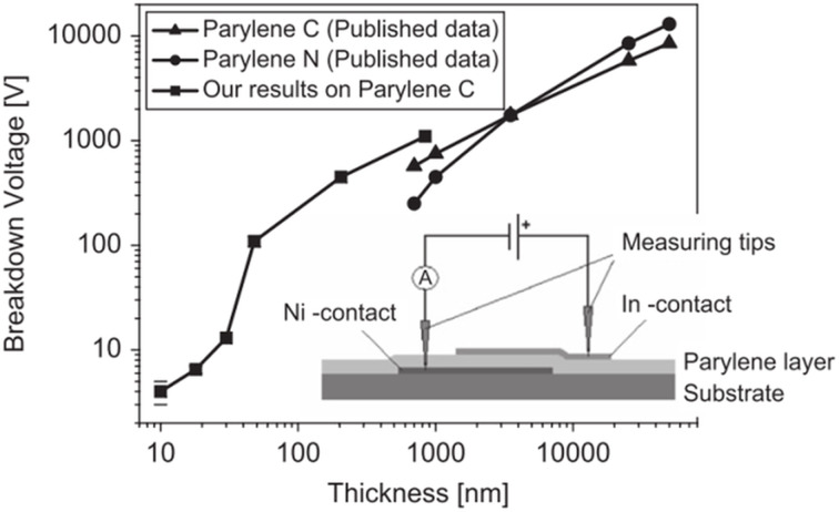
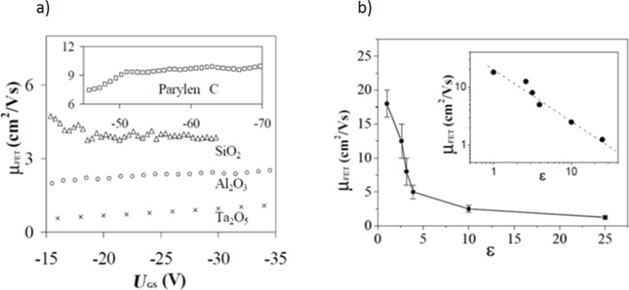
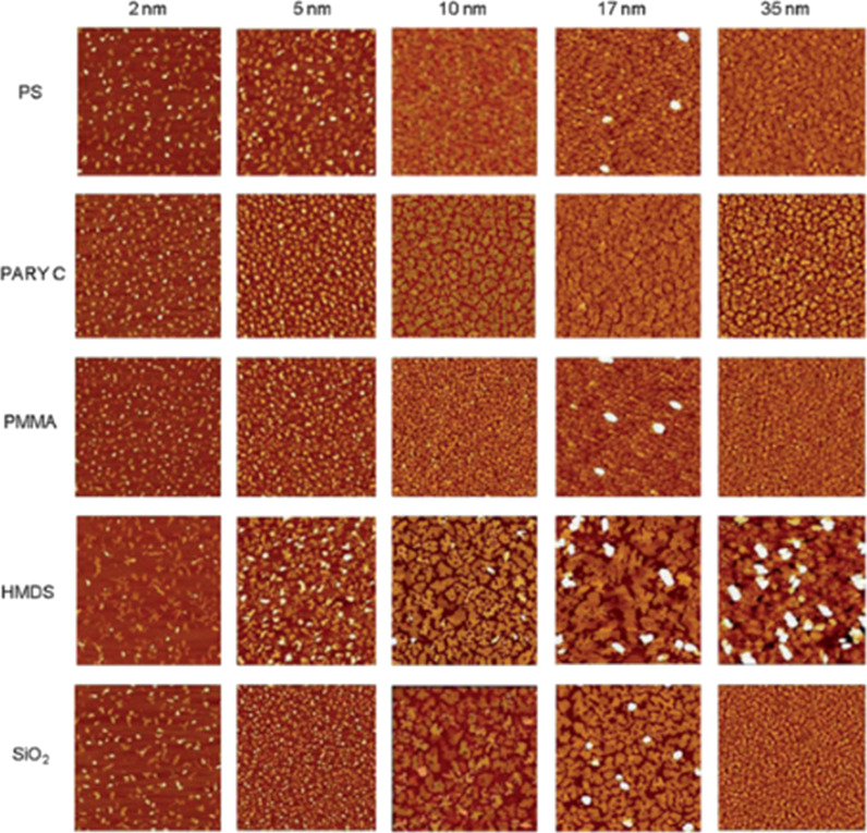
An emerging new technology, organic electronics, is approaching the stage of large-scale industrial application. This is due to a remarkable progress in synthesis of a variety of organic semiconductors, allowing one to design and to fabricate, so far on a laboratory scale, different organic electronic devices of satisfactory performance. However, a complete technology requires upgrading of fabrication procedures of all elements of electronic devices and circuits, which not only comprise active layers, but also electrodes, dielectrics, insulators, substrates and protecting/encapsulating coatings. In this review, poly(chloro-para-xylylene) known as Parylene C, which appears to become a versatile supporting material especially suitable for applications in flexible organic electronics, is presented. A synthesis and basic properties of Parylene C are described, followed by several examples of use of parylenes as substrates, dielectrics, insulators, or protecting materials in the construction of organic field-effect transistors.

Keywords: Parylene C; dielectric; encapsulation layer; flexible substrate; organic field effect transistor.


Figures

Figure 1
Figure 1
Schematic representation of the deposition process of Parylene C with the respective chemical reactions. Reprinted with permission from [28], copyright 2016 Elsevier.
Figure 2
Figure 2
AFM measurements of the surface roughness of Parylene C thin films. Reprinted with permission from [30], copyright 2009 Elsevier.
Figure 3
Figure 3
XRD spectra of Parylene C films: as-deposited with constant deposition rate and thermally annealed at different temperatures (a), as-deposited with different deposition rates and thermally annealed at constant temperature (b). Reprinted with permission from [29] copyright 2008 MYU K.K. (reprinted from electronic version).
Figure 4
Figure 4
Schematic illustration of the flexible OFET fabrication procedure with Parylene C as a substrate and gate dielectric layer and with zone-cast tetrakis(alkylthio)tetrathiafulvalene as semiconductor. Reprinted with permission from [34].
Figure 5
Figure 5
Transfer characteristics of 10 OTFTs after bending and crumpling tests: (a) Photograph of a device before mechanical tests. (b) Photograph of a device rolled onto a cylinder of 0.8 mm radius. (c) Photograph of a crumpled device. (d) and (e) Transfer characteristics of 10 OTFTs before and after bending and crumpling tests. Reprinted with permission from [33] copyright 2016 IOP Publishing Ltd.
Figure 6
Figure 6
Thin Parylene C layers breakdown voltage as a function of thickness. Reprinted with permission from [30], copyright 2009 Elsevier.
Figure 7
Figure 7
(a) Mobility μ(Vg) curves measured for four different gate insulators. For the device based on Parylene C, the suppression of contact effects often requires a rather large value of VDS (and thus VGS) to remain in the linear regime. (b) Decrease of the mobility with increasing ε, as observed in rubrene single-crystal FETs with different gate insulators. The bars give a measure of the spread in mobility values. Inset: when plotted on a log–log scale, the available data show a linear dependence with slope −1 (i.e., the variation in μ is proportional to ε−1). Reprinted with permission from [37], copyright 2004 of AIP Publishing.
Figure 8
Figure 8
10 μm × 10 μm AFM images of tetracene thin films on different dielectric surfaces at different nominal thickness. Z-scale: 50 nm. Reprinted with permission from [50], copyright 2013 Royal Society of Chemistry.
Figure 9
Figure 9
(a) Transistor architecture of the three different transistor stacks investigated, (b) threshold voltage trends of successive transfer sweeps for different VD, (c) representative transfer IV characteristics of the three transistor stacks. The arrows in (c) indicate the sweeping direction of VG. Reprinted with permission from [51], copyright 2016 Springer.
Figure 10
Figure 10
Transfer characteristics measured during the continuous bias stress of 125 h. (a) Bottom-gate, top-contacts, (b) top-gate, bottom-contacts, and (c) dual-gate OFETs. Reprinted from [54], copyright 2014 American Chemical Society.
Figure 11
Figure 11
Volumetric reconstruction of the Parylene C-coated microscopy glass (left, atop) and calculated amplitude map of the Parylene C/glass interface (left, bottom). Boundary box indicates the size of the volume 2000 × 2000 × 208 µm. Zoom-in image (right). Coating defects and gas chambers are clearly visible. Reprinted with the permission from [68], copyright 2011 Springer.
Figure 12
Figure 12
Volumetric reconstruction of the Parylene C-coated OFET structure (left, atop) and calculated amplitude map of the Parylene C/substrate interface (left, bottom). Boundary box indicates the size of the volume 2000 × 2000 × 73 µm. Zoom-in image showing interfaces of 2 µm thin polymer layer (right). Reprinted with the permission from [68], copyright 2011 Springer.
Figure 13
Figure 13
Transfer characteristics recorded under ambient conditions of a fullerene transistor without encapsulation (a), encapsulated with 1 μm thick layer of Parylene C (b) and encapsulated with 0.5 μm thick layer of Parylene C followed by 0.5 μm layer of benzocyclobutene (c). Reprinted with the permission from [69], copyright 2014 Elsevier.

References

    1. Xu X, Yao Y, Shan B, Gu X, Liu D, Liu J, Xu J, Zhao N, Hu W, Miao Q. Adv Mater. 2016;28:5276–5283. doi: 10.1002/adma.201601171. - DOI - PubMed
    1. Podzorov V, Pudalov V M, Gershenson M E. Appl Phys Lett. 2003;82:1739–1741. doi: 10.1063/1.1560869. - DOI
    1. Yamashita Y, Hinkel F, Marszalek T, Zajaczkowski W, Pisula W, Baumgarten M, Matsui H, Müllen K, Takeya J. Chem Mater. 2016;28:420–424. doi: 10.1021/acs.chemmater.5b04567. - DOI
    1. Marszalek T, Li M, Pisula W. Chem Commun. 2016;52:10938–10947. doi: 10.1039/C6CC04523E. - DOI - PubMed
    1. Zhang H, Guo X, Hui J, Hu S, Xu W, Zhu D. Nano Lett. 2011;11:4939–4946. doi: 10.1021/nl2028798. - DOI - PubMed

LinkOut - more resources