Review
. 2017 Jul 10:8:1407-1426.
doi: 10.3762/bjnano.8.142. eCollection 2017.

A review of demodulation techniques for amplitude-modulation atomic force microscopy

Affiliations
Review

A review of demodulation techniques for amplitude-modulation atomic force microscopy

Michael G Ruppert et al. Beilstein J Nanotechnol. .

Abstract

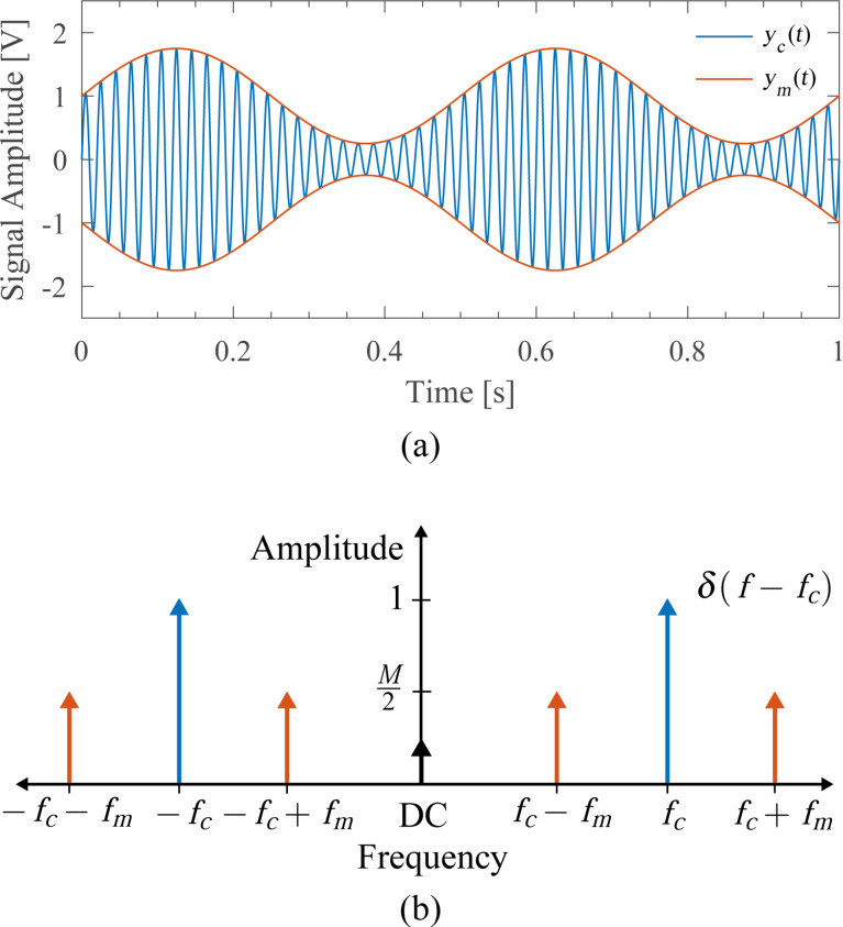
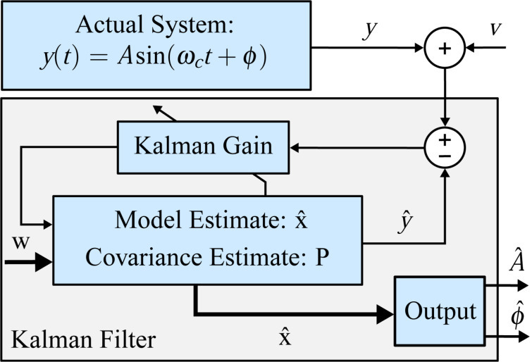
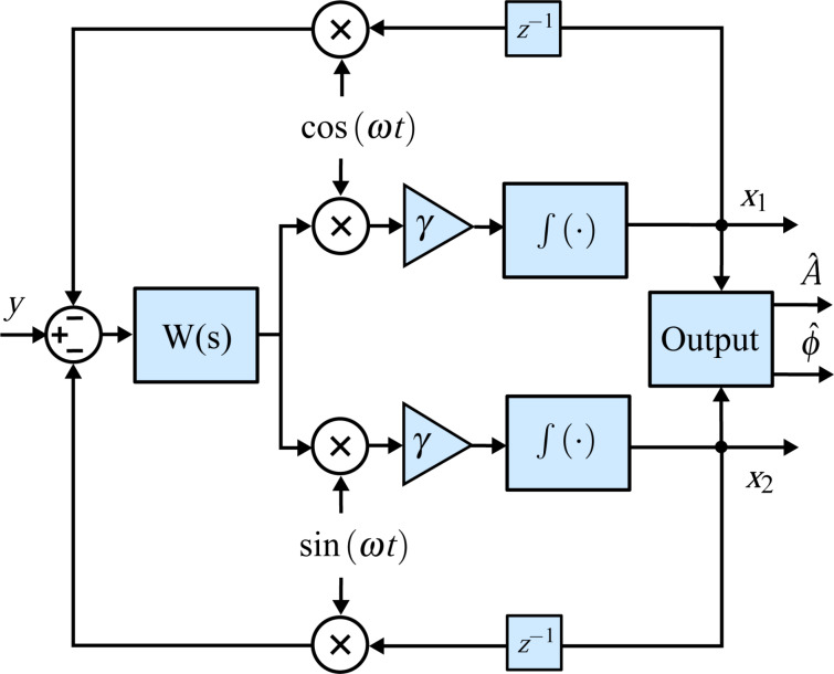
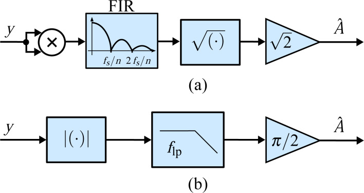
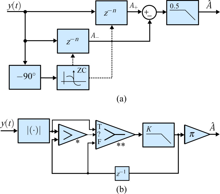
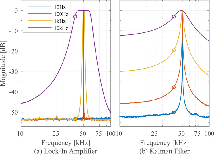
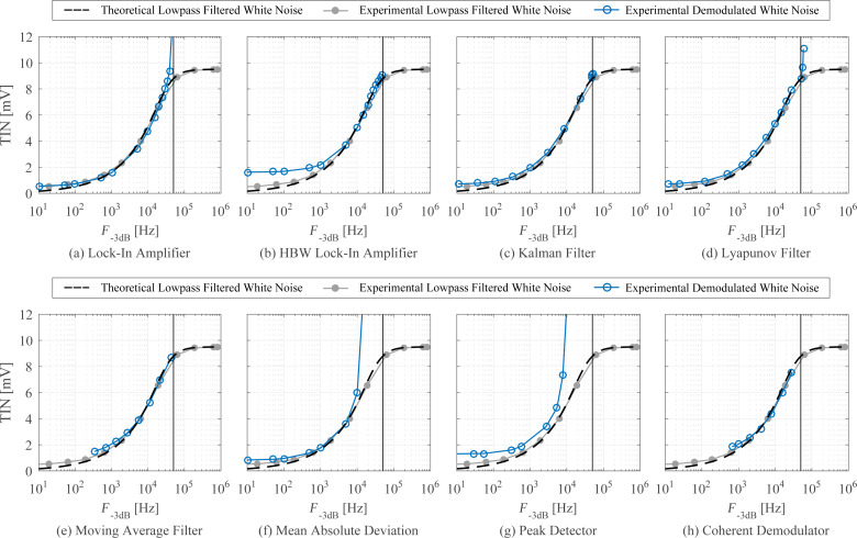
In this review paper, traditional and novel demodulation methods applicable to amplitude-modulation atomic force microscopy are implemented on a widely used digital processing system. As a crucial bandwidth-limiting component in the z-axis feedback loop of an atomic force microscope, the purpose of the demodulator is to obtain estimates of amplitude and phase of the cantilever deflection signal in the presence of sensor noise or additional distinct frequency components. Specifically for modern multifrequency techniques, where higher harmonic and/or higher eigenmode contributions are present in the oscillation signal, the fidelity of the estimates obtained from some demodulation techniques is not guaranteed. To enable a rigorous comparison, the performance metrics tracking bandwidth, implementation complexity and sensitivity to other frequency components are experimentally evaluated for each method. Finally, the significance of an adequate demodulator bandwidth is highlighted during high-speed tapping-mode atomic force microscopy experiments in constant-height mode.

Keywords: amplitude estimation; amplitude modulation; atomic force microscopy; digital signal processing; field-programmable gate array.


Figures

Figure 1
Figure 1
(a) Time-domain example of an amplitude modulated signal with carrier frequency fc = 50 Hz, modulating frequency fm = 5 Hz, and modulation index M = 0.75 and (b) its double-sided amplitude spectrum. A small residual DC offset is also shown for the sake of completeness.
Figure 2
Figure 2
Classification of demodulation methods discussed in this paper.
Figure 3
Figure 3
(a) Functional block diagram of the lock-in amplifier implementation and (b) illustrative double-sided amplitude spectrum of the signal after mixing.
Figure 4
Figure 4
(a) Functional block diagram of the high-bandwidth lock-in amplifier implementation and (b) illustrative double-sided amplitude spectrum of the signal after the summing stage.
Figure 5
Figure 5
General block diagram of the Kalman filter for demodulation. Thick lines indicate vector-valued signal paths and thin lines indicate scalar signal paths.
Figure 6
Figure 6
Functional block diagram of the Lyapunov filter implementation.
Figure 7
Figure 7
Functional block diagram of (a) moving average filter and (b) mean absolute deviation measurement to perform digital RMS-to-DC conversion.
Figure 8
Figure 8
Functional block diagram of (a) the peak hold method and (b) the modified peak hold method based on a peak detector implementation alleviating the sample frequency limitation. The blocks labeled * and ** follow the LabVIEW-specific layout and represent the “greater” and triggered selector functionality.
Figure 9
Figure 9
Functional block diagram of the coherent demodulator implementation.
Figure 10
Figure 10
Schematic signal flow of the numerical integration scheme employed by the coherent demodulator with and without post-integration filter. Since formula image
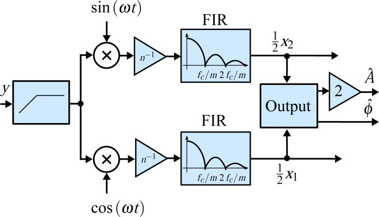
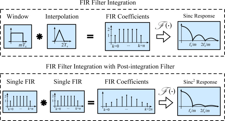
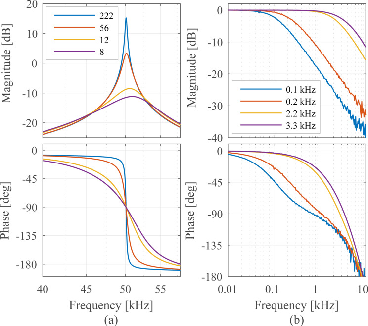
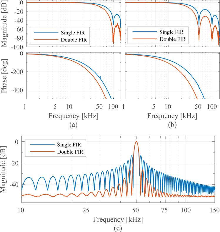
, the frequency response of the interpolation filter can be neglected.
Figure 11
Figure 11
Tracking bandwidth frequency response of the demodulators showing the −3 dB tracking bandwidth and equivalent filter order for four different bandwidth settings each.
Figure 12
Figure 12
Off-mode rejection of the demodulators for a carrier frequency of fc = 50 kHz and a tracking bandwidth of 1 kHz. The zoom box highlights the intersection at the points (50 ± 1 kHz, −3 dB) and the different filter shapes at the modeled carrier frequency.
Figure 13
Figure 13
Off-mode rejection of (a) fourth-order lock-in amplifier and (b) first-order Kalman filter for a carrier frequency of fc = 50 kHz at 10 Hz, 100 Hz, 1 kHz, and 10 kHz tracking bandwidth.
Figure 14
Figure 14
Schematic block diagram of the reference experiment of filtering a band-limited white noise process with a variable cut-off frequency low-pass filter and its schematic representation in the frequency domain.
Figure 15
Figure 15
Schematic block diagram of bandwidth-vs-noise experiment of recovering an amplitude-modulated band-limited white noise process with demodulators with variable tracking bandwidths and its schematic representation in the frequency domain.
Figure 16
Figure 16
Tracking bandwidth vs total integrated noise (TIN) for each demodulator (blue circles) and for a low-pass filtered white noise process (gray dots) and its analytical expression (dashed black line) as reference. The vertical line indicates the location of the carrier frequency fc = 50 kHz.
Figure 17
Figure 17
(a) Frequency response of the DMASP cantilever in open-loop (blue) and for various quality factor controller gains to reduce the quality factor as stated in the legend. (b) Tracking bandwidths of the DMASP cantilever determined via drive amplitude modulation for the frequency responses shown in (a) and color-coded accordingly.
Figure 18
Figure 18
3D image, 2D image and cross section of amplitude estimates obtained from (a) lock-in amplifier with flp = 100 Hz, (b) lock-in amplifier with flp = 200 Hz, and (c) Lyapunov filter with γ = 60000 at an imaging speed of 627.45 μm/s. The scanning direction is along the positive x- and y-axes.
Figure 19
Figure 19
3D image, 2D image and cross section of amplitude estimates obtained from (a) lock-in amplifier with flp = 200 Hz, (b) lock-in amplifier with flp = 300 Hz, and (c) Kalman filter with Q = 0.004, R = 2 at an imaging speed of 1.25 mm/s. The scanning direction is along the positive x- and y-axes.
Figure 20
Figure 20
Functional block diagram of the Kalman filter implementation. Thick lines indicate vector-valued signal paths and thin lines indicate scalar signal paths.
Figure 21
Figure 21
Maximum tracking bandwidth of (a) coherent demodulator (n = 6) and (b) half-period coherent demodulator (n = 3) with single FIR integration filter (blue) and FIR integration filter with post-integration filter (red). (c) Off-mode rejection at 1 kHz tracking bandwidth of coherent demodulator with single FIR integration filter (blue) and FIR integration filter with post-integration filter (red) using fs = 300 kHz, fc = 50 kHz.
Figure 22
Figure 22
Relationship between demodulator tuning variable and achievable tracking bandwidth.
Figure 23
Figure 23
Experimental and theoretical total integrated noise of a low-pass filtered white noise process for a first-order system G1 and a second-order system G2. The experimental data was fitted to Equation 26 and Equation 29 using nonlinear least squares.

Similar articles

Cited by

References

    1. Haykin S. Communication systems. John Wiley & Sons; 2008.
    1. Nyce D S. Linear position sensors: theory and application. John Wiley & Sons; 2004.
    1. Baxter L K. Capacitive sensors: Design and Applications. Wiley-IEEE Press; 1996.
    1. Fleming A J. Sens Actuators, A. 2013;190:106–126. doi: 10.1016/j.sna.2012.10.016. - DOI
    1. Tsui D C, Stormer H L, Gossard A C. Phys Rev Lett. 1982;48:1559–1562. doi: 10.1103/PhysRevLett.48.1559. - DOI