. 2017 Sep 21;8(1):633.
doi: 10.1038/s41467-017-00734-x.

Short-channel field-effect transistors with 9-atom and 13-atom wide graphene nanoribbons

Affiliations

Short-channel field-effect transistors with 9-atom and 13-atom wide graphene nanoribbons

Juan Pablo Llinas et al. Nat Commun. .

Abstract

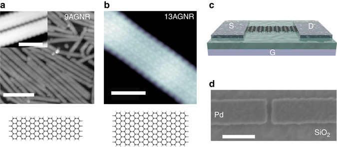
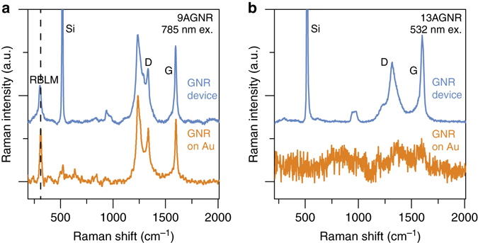
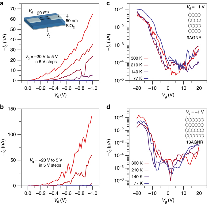
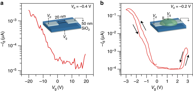
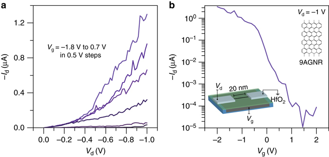
Bottom-up synthesized graphene nanoribbons and graphene nanoribbon heterostructures have promising electronic properties for high-performance field-effect transistors and ultra-low power devices such as tunneling field-effect transistors. However, the short length and wide band gap of these graphene nanoribbons have prevented the fabrication of devices with the desired performance and switching behavior. Here, by fabricating short channel (L ch ~ 20 nm) devices with a thin, high-κ gate dielectric and a 9-atom wide (0.95 nm) armchair graphene nanoribbon as the channel material, we demonstrate field-effect transistors with high on-current (I on > 1 μA at V d = -1 V) and high I on /I off ~ 105 at room temperature. We find that the performance of these devices is limited by tunneling through the Schottky barrier at the contacts and we observe an increase in the transparency of the barrier by increasing the gate field near the contacts. Our results thus demonstrate successful fabrication of high-performance short-channel field-effect transistors with bottom-up synthesized armchair graphene nanoribbons.Graphene nanoribbons show promise for high-performance field-effect transistors, however they often suffer from short lengths and wide band gaps. Here, the authors use a bottom-up synthesis approach to fabricate 9- and 13-atom wide ribbons, enabling short-channel transistors with 105 on-off current ratio.


Conflict of interest statement

The authors declare no competing financial interests.

Figures

Fig. 1
Fig. 1
High-resolution STM GNR characterization and FET structure. a STM image of synthesized 9AGNR on Au with a scale bar of 10 nm (V s = 1 V, I t = 0.3 nA). Inset: High-resolution STM image of 9AGNR on Au (V s = 1 V, I t = 0.5 nA) with a scale bar of 1 nm. b High-resolution STM image of 13AGNR on Au with a scale bar of 2 nm (V s = −0.7 V, I t = 7 nA). c Schematic of the short channel GNRFET with a 9AGNR channel and Pd source-drain electrodes. d Scanning electron micrograph of the fabricated Pd source-drain electrodes with a scale bar of 100 nm
Fig. 2
Fig. 2
Raman spectra of as-grown GNRs on Au and GNRs after transfer and device processing. Raman spectra of a 9AGNRs and b 13AGNRs on the Au(111) growth substrate and after device fabrication shows that the GNRs remain intact. Since the excitation is off-resonance with the 13AGNR absorption, the Raman signal is weak on Au and the RBLM is not visible
Fig. 3
Fig. 3
Transport characteristics of 9AGNRs and 13AGNRs gated with 50 nm SiO2 gate oxide. The presence of a SB is confirmed by non-linear current behavior at low drain bias and lack of current saturation at high drain bias for both a 9AGNRs and b 13AGNRs. The weak temperature dependence in the I d −V g behavior in c 9AGNRs and d 13AGNRs indicates that tunneling through the Pd-GNR SBs is the limiting transport mechanism of the device
Fig. 4
Fig. 4
Ionic liquid gating of a 9AGNRFET at room temperature. a I d −V g characteristics of the device gated by the thick 50 nm SiO2 gate oxide. b I d −V g characteristics of the device gated with the ionic liquid which shows clear ambipolar behavior and improved on-state performance. Inset: ionic liquid (DEME-TFSI) gated 9AGNRFET device schematic
Fig. 5
Fig. 5
Transport characteristics of a scaled, high-performance 9AGNRFET at room temperature. a I d −V d characteristics of the scaled 9AGNRFET. b I d −V g of the devices show high I on > 1 μA for a 0.95 nm wide 9AGNR and high I on /I off ~ 105. Inset: scaled 9AGNRFET schematic

References

    1. Cai J, et al. Atomically precise bottom-up fabrication of graphene nanoribbons. Nature. 2010;466:470–473. doi: 10.1038/nature09211. - DOI - PubMed
    1. Chen Y-C, et al. Tuning the band gap of graphene nanoribbons synthesized from molecular precursors. ACS Nano. 2013;7:6123–6128. doi: 10.1021/nn401948e. - DOI - PubMed
    1. Narita A, et al. Synthesis of structurally well-defined and liquid-phase-processable graphene nanoribbons. Nat. Chem. 2014;6:126–132. doi: 10.1038/nchem.1819. - DOI - PubMed
    1. Narita A, Wang X-Y, Feng X, Müllen K. New advances in nanographene chemistry. Chem. Soc. Rev. 2015;44:6616–6643. doi: 10.1039/C5CS00183H. - DOI - PubMed
    1. Ruffieux P, et al. On-surface synthesis of graphene nanoribbons with zigzag edge topology. Nature. 2016;531:489–492. doi: 10.1038/nature17151. - DOI - PubMed

Publication types