. 2017 Sep 22;7(1):12154.
doi: 10.1038/s41598-017-12447-8.

Exchange-driven Magnetic Logic

Affiliations

Exchange-driven Magnetic Logic

Odysseas Zografos et al. Sci Rep. .

Abstract

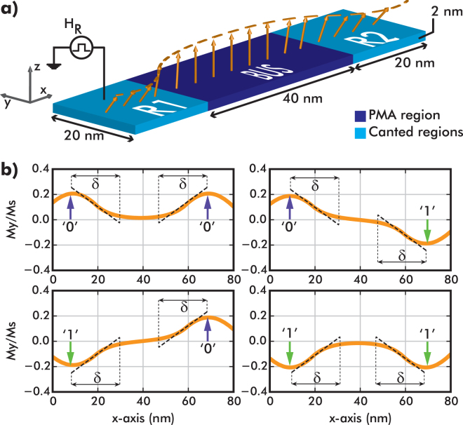
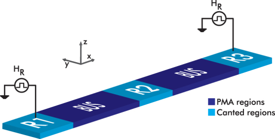
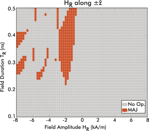
Direct exchange interaction allows spins to be magnetically ordered. Additionally, it can be an efficient manipulation pathway for low-powered spintronic logic devices. We present a novel logic scheme driven by exchange between two distinct regions in a composite magnetic layer containing a bistable canted magnetization configuration. By applying a magnetic field pulse to the input region, the magnetization state is propagated to the output via spin-to-spin interaction in which the output state is given by the magnetization orientation of the output region. The dependence of this scheme with input field conditions is extensively studied through a wide range of micromagnetic simulations. These results allow different logic operating modes to be extracted from the simulation results, and majority logic is successfully demonstrated.


Conflict of interest statement

The authors declare that they have no competing interests.

Figures

Figure 1
Figure 1
(a) The structure consists of an input (R1) and an output (R2) magnetic regions connected through a ferromagnetic bus. The length of the bus region is 40 nm. (b) Four possible initial magnetization states of the structure’s magnetization canted along the y-direction in the absence of any external field. The magnetization state of the R1 and R2 regions are represented by ‘0’ (if My/Ms0.2) or ‘1’ (My/Ms0.2).
Figure 2
Figure 2
(a) Applied triggering field’s H R = 0 direction. Magnetization dynamics of input (R1 - blue) and output (R2 - green) regions. Insets: projection of the output magnetization onto the xy-plane (b) when T R = 0.2 ns: the output does not switch to state 1, (c) when T R = 0.5 ns: the output does switch from state 0 to 1.
Figure 3
Figure 3
Evolution of My/Ms projected on xˆ-axis over time. Input field appled is H R = 8 kA/m and T R = 0.5 ns.
Figure 4
Figure 4
Acting torques on input (R1) and output (R2) regions as a function of time, calculated by Eq. 1. (a) xˆ-component of the exchange torque. (b) yˆ-component of the exchange torque. (c) xˆ -component of the demagnetization torque. (d) yˆ-component of the demagnetization torque.
Figure 5
Figure 5
(a) Phase diagram of the operating regions (i.e. mode M1) as a function of input amplitude and duration. The input field is applied along the y-axis. (b) Phase diagram of the operating regions (when the output switches) versus the input amplitude and duration when input is applied along-zˆ. Inverter mode (orange) represents the cases (0X HRX1, 1X HRX0). Buffer mode (cyan) represents the cases (0X HRX0, 1X HRX1).
Figure 6
Figure 6
Majority gate structure of exchange-driven magnetic logic. The initial canted magnetization states of regions R1, R2, R3 are considered the three inputs of the gate. Two triggering magnetic pulses are applied at regions R1 and R3 and the sum of all three contributions result in R2 having the result of the gate.
Figure 7
Figure 7
Phase diagram of the Majority gate operating regions (when the R2 regions switches to the correct majority result) of the input amplitude and duration, when fields are applied along zˆ. In the majority gate two triggering fields are applied and both are swept simultaneously.
Figure 8
Figure 8
(a) Example circuit with two cascaded majority gates. (b) Translated circuit to accommodate the exchange-driven logic structures. (c) Triggering field pulses applied at each region (R1 to R6) of the structure to implement either the majority or inverter operation. (d) Normalized magnetization along yˆ-axis over time for each of the regions of the structures. My/Ms0.2 is represented by ‘0’ and My/Ms0.2 is represented by ‘1’. (e) Schematic showing the magnetization states of the structure at different time points of the entire circuit operation.
Figure 9
Figure 9
(a) Schematic of rectangular TiN layer that introduces residual strain along the yˆ-axis. (b) Schematic of material stack that allows application of triggering voltages and integration with other CMOS components.

References

    1. Hutchby J, Bourianoff G, Zhirnov V, Brewer J. Extending the road beyond cmos. IEEE Circuits and Devices Magazine. 2002;18:28. doi: 10.1109/101.994856. - DOI
    1. Moore G. Cramming more components onto integrated circuits. Electronics. 1965;38:114.
    1. Zhirnov V, Cavin R, Hutchby J, Bourianoff G. Limits to binary logic switch scaling - a gedanken model. Proceedings of the IEEE. 2003;9:1934. doi: 10.1109/JPROC.2003.818324. - DOI
    1. Nikonov DE, Young I. Overview of beyond-cmos devices and a uniform methodology for their benchmarking. Proceedings of the IEEE. 2013;101:2498. doi: 10.1109/JPROC.2013.2252317. - DOI
    1. Bernstein K, Cavin RK, Porod W, Seabaugh A, Welser J. Device and architecture outlook for beyond cmos switches. Proceedings of the IEEE. 2010;98:2169. doi: 10.1109/JPROC.2010.2066530. - DOI