. 2017 Oct 19;17(10):2388.
doi: 10.3390/s17102388.

Time Multiplexed Active Neural Probe with 1356 Parallel Recording Sites

Affiliations

Time Multiplexed Active Neural Probe with 1356 Parallel Recording Sites

Bogdan C Raducanu et al. Sensors (Basel). .

Abstract

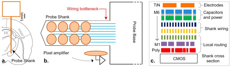
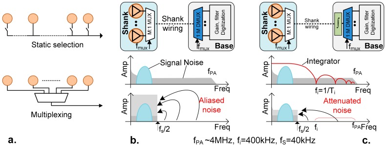
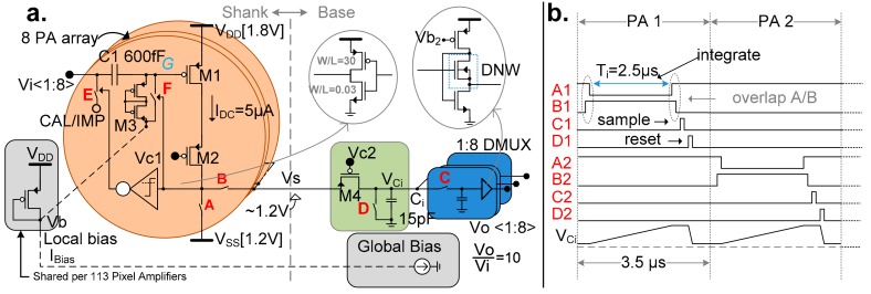
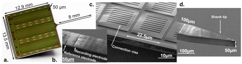
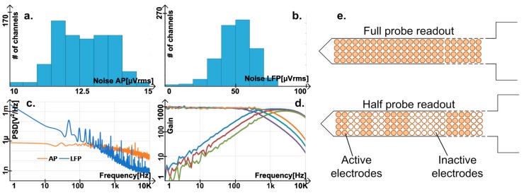
We present a high electrode density and high channel count CMOS (complementary metal-oxide-semiconductor) active neural probe containing 1344 neuron sized recording pixels (20 µm × 20 µm) and 12 reference pixels (20 µm × 80 µm), densely packed on a 50 µm thick, 100 µm wide, and 8 mm long shank. The active electrodes or pixels consist of dedicated in-situ circuits for signal source amplification, which are directly located under each electrode. The probe supports the simultaneous recording of all 1356 electrodes with sufficient signal to noise ratio for typical neuroscience applications. For enhanced performance, further noise reduction can be achieved while using half of the electrodes (678). Both of these numbers considerably surpass the state-of-the art active neural probes in both electrode count and number of recording channels. The measured input referred noise in the action potential band is 12.4 µVrms, while using 678 electrodes, with just 3 µW power dissipation per pixel and 45 µW per read-out channel (including data transmission).

Keywords: CMOS; active electrode; active neural probes; high density component; neural amplifier; neural array; neural recording.


Conflict of interest statement

The authors declare no conflict of interest.

Figures

Figure 1
Figure 1
(a) Schematic of implanted probe reaching multiple areas inside a rat brain; (b) neural probe with shank wiring bottleneck limiting the number of electrodes; (c) typical CMOS (complementary metal-oxide-semiconductor) back end-of-line cross section, with six metal layers.
Figure 2
Figure 2
(a) Traditional approach (top) employs a static switch which allows only a single active electrode to be read at the same time, while the new approach (bottom) allows all of the active electrodes to be readout through multiplexing; (b) consequences of multiplexing without filtering; (c) filtering signal by integration reduces out-of-band thermal noise.
Figure 3
Figure 3
(a) Normalized power density across the shank due to increasing current and supply towards the base; (b) thermal simulations of probe with holder implanted in the brain, showing maximum temperature of 38 °C reached at the edge of the brain. This simulation was used to determine the maximum safe power that may be dissipated in the shank.
Figure 4
Figure 4
(a) Probe architecture showing the device contains one channel for each electrode; left: the recording and reference electrodes on the probe and their corresponding signal blocks; (b) Channel details showing (symbolically) the electrode connections and reference selection options available on each channel (2 local, external or ground); an averaging line is used to connect any of the 12 local reference together and average the signal across them; the amplification section consists of AC (alternating current) coupled instrumentation amplifier (IA) and programmable gain amplifier (PGA), along with configurable band selection and cutoff corner filter.
Figure 5
Figure 5
(a) Pixel amplifiers (PA) architecture: M1 works as gm stage. The cascode transistor M2 isolates M1 from the clock feedthrough at the output and overlapped A/B switches enable M1 to always have an ON current. Both these methods along with proper layout placement ensure the stability of high impedance node G. The S/H circuit uses flipped voltage follower buffer with a deep N-well NMOS; (b) timing diagram showing the switching cycles of 2 consecutive PAs.
Figure 6
Figure 6
(a) Large supply drop across the 8 mm long shank changes the bias voltage, ΔVb. This is due to the high current in the supply rail (consumed by all PAs), that causes voltage drop within a bias region (ΔVDDG); (b) a tree-like power supply ensures that supply change ΔVDL is close to zero within each region, due to the lower current in the local rail. Each region contains its dedicated local bias generator.
Figure 7
Figure 7
(a) Chip microphotograph showing complete probe with base and shank; (b) shank detail of small 20 µm × 20 µm and reference 40 µm × 80 µm electrodes; (c) detail of electrodes showing titanium nitride vias connecting the electrode to the internal metals and (d) details of the sharp shank tip and dimensions.
Figure 8
Figure 8
(a) Probe testing in saline solution attached to headstage, showing the back-end FPGA board in the background; (b) detailed view of probe and headstage connected to the mezzanine PCB (printed circuit board) through the flexible dual micro coaxial cable; the mezzanine board allows for connection of external battery for low noise and digital synchronization signals; (c) schematic display of probe implanted into animal.
Figure 9
Figure 9
Adapted from [5]. Measurement results in half-probe readout, omitting the small number of defective channels; (a) distribution of noise in AP and (b) LFP band; (c) noise density in AP band (300 Hz–7.5 kHz) and LFP band (1 Hz–1 kHz); (d) different filter corner configurations, considering a fixed total gain of 1000; LFP high pass corners is below 1 Hz and not visible; (e) full probe readout and half probe readout allowing 6 random regions out of 12 to be active.
Figure 10
Figure 10
(a) local field potentials (LFP) simultaneously recorded from the neocortex (red), hippocampus (green), and thalamus (blue). Traces were obtained from the raw data recorded in LFP mode (internal reference, gain 500, low-pass 500 Hz); (b) multi- and single-unit activity recorded simultaneously from the neocortex (red), hippocampus (green), and thalamus (blue). Traces were recorded in action potentials (AP) mode (internal reference, gain 1000, high-pass 500 Hz). Dashed and dotted box indicate neocortical/thalamic up-states (U) and down-states (D); (c) schematic of a coronal rat brain section indicating the estimated position of neural recordings, d. fast Fourier Transform (FFT) plot of the recorded neural activity showing the dominant brain rhythms in the investigated brain areas during ketamine/xylazine anesthesia. Note that slow wave activity (1–1.5 Hz) appeared in all three brain structures, while high gamma activity (30–40 Hz) was present only in the hippocampus.
Figure 11
Figure 11
Representative spiking activity across more than 1250 channels of the probe shank, spanning approximately 7.5 mm of brain tissue. The raw data is shown. The spike-map was constructed from 1 second of data recorded in AP mode; the time series of each channel’s data is plotted as a horizontal line using brightness to encode the absolute amplitude, with darker areas being an indication of neural spiking activity. Ketamine/xylazine anesthesia induces slow wave activity (with a peak frequency of 1–1.5 Hz) or delta rhythm (1.5–4 Hz) in the neocortex and thalamus, which can be observed as a rhythmic alternation of high and low spiking activity. Notes: the first ~90 channels are not displayed as they were outside of the brain and only recorded noise; the picture requires one line per channel (~1250), therefore resolution of the provided image was scaled down. Occasionally neurons near the reference electrode may spike, causing a line to be displayed on all channels using that specific local reference. Such artefacts can be eliminated during offline processing.
Figure 12
Figure 12
Cluster quality metrics (isolation distance and refractory period violations) calculated for single units recorded with the CMOS probe (n = 247) and with passive silicon probes (n = 101). Red line: median; blue box: 1st quartile–3rd quartile; whiskers: 1.5× interquartile range above and below the box; green dots: outliers. Extreme outliers are not displayed (isolation distance: 12 data points from the CMOS probe data ranging from 183 to 475; refractory period violations: 22 data points from the CMOS probe data ranging from 2.2 to 13.1 percent and 3 data points from the passive silicon probe data ranging from 2.8 to 4.2 percent). **: p < 0.01; ***: p < 0.001.
Figure 13
Figure 13
(a) The mean spike waveforms of a putative neocortical pyramidal cell captured on 4 × 14 electrodes. The waveform with the largest peak-to-peak amplitude is colored red; (b) individual spikes (waveforms in gray color, n = 90) of the same pyramidal cell recorded by the electrode corresponding to the red waveform in panel a. The mean spike waveform is displayed in red color; (c) the autocorrelogram of the demonstrated pyramidal neuron (bin size: 1 ms). The two peaks indicate burst firing (multiple spikes fired in rapid succession); (d) Color-coded potential distribution maps corresponding to different time points of the mean spike waveform. The maps are visualized according to the layout of the 4 × 14 electrodes. The potential map corresponding to the time point of the negative peak of the mean spike waveform shown in panel b is indicated with an asterisk. Note the temporal propagation of the negative peak of the spike (red patch) from lower electrodes to upper electrodes. The spikes of the neuron were recorded in AP mode (internal reference, gain 500, high-pass 500 Hz).

References

    1. Buzsáki G., Stark E., Berényi A., Khodagholy D., Kipke D.R., Yoon E., Wise K.D. Tools for probing local circuits: High-density silicon probes combined with optogenetics. Neuron. 2015;86:92–105. doi: 10.1016/j.neuron.2015.01.028. - DOI - PMC - PubMed
    1. Lopez C.M., Andrei A., Mitra S., Welkenhuysen M., Eberle W., Bartic C., Puers R., Yazicioglu R.F., Gielen G.G.E. An Implantable 455-Active-Electrode 52-Channel CMOS Neural Probe. IEEE J. Solid-State Circuits. 2014;49:248–261. doi: 10.1109/JSSC.2013.2284347. - DOI
    1. Olsson R.H., Wise K.D. A three-dimensional neural recording microsystem with implantable data compression circuitry. IEEE J. Solid-State Circuits. 2005;40:2796–2804. doi: 10.1109/JSSC.2005.858479. - DOI
    1. Lopez C.M., Putzeys J., Raducanu B.C., Ballini M., Wang S., Andrei A., Rochus V., Vandebriel R., Severi S., Van Hoof C., et al. A neural probe with up to 966 electrodes and up to 384 configurable channels in 0.13 µm SOI CMOS. IEEE Trans. Biomed. Circuits Syst. 2017;11:510–522. doi: 10.1109/TBCAS.2016.2646901. - DOI - PubMed
    1. Raducanu B.C., Yazicioglu R.F., Lopez C.M., Ballini M., Putzeys J., Wang S., Andrei A., Welkenhuysen M., van Helleputte N., Musa S., et al. Time multiplexed active neural probe with 678 parallel recording sites; Proceedings of the 2016 46th European Solid-State Device Research Conference (ESSDERC); Lausanne, Switzerland. 12–15 September 2016; pp. 385–388.