. 2017 Nov 28;11(11):11661-11668.
doi: 10.1021/acsnano.7b06765. Epub 2017 Oct 25.

Width-Dependent Band Gap in Armchair Graphene Nanoribbons Reveals Fermi Level Pinning on Au(111)

Affiliations

Width-Dependent Band Gap in Armchair Graphene Nanoribbons Reveals Fermi Level Pinning on Au(111)

Néstor Merino-Díez et al. ACS Nano. .

Abstract

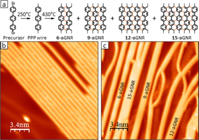
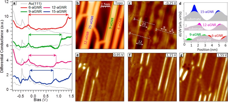
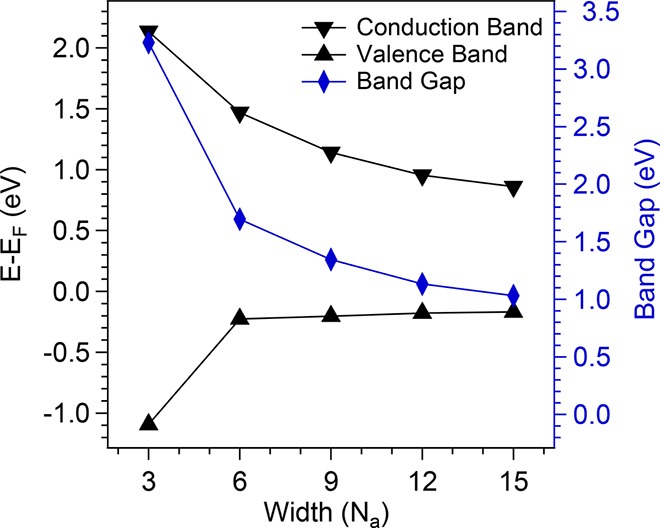
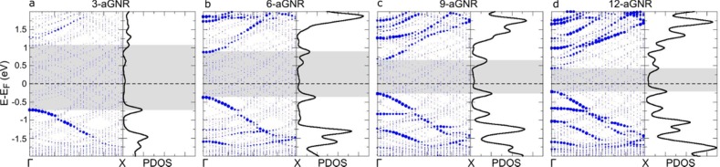
We report the energy level alignment evolution of valence and conduction bands of armchair-oriented graphene nanoribbons (aGNR) as their band gap shrinks with increasing width. We use 4,4″-dibromo-para-terphenyl as the molecular precursor on Au(111) to form extended poly-para-phenylene nanowires, which can subsequently be fused sideways to form atomically precise aGNRs of varying widths. We measure the frontier bands by means of scanning tunneling spectroscopy, corroborating that the nanoribbon's band gap is inversely proportional to their width. Interestingly, valence bands are found to show Fermi level pinning as the band gap decreases below a threshold value around 1.7 eV. Such behavior is of critical importance to understand the properties of potential contacts in GNR-based devices. Our measurements further reveal a particularly interesting system for studying Fermi level pinning by modifying an adsorbate's band gap while maintaining an almost unchanged interface chemistry defined by substrate and adsorbate.

Keywords: Fermi level pinning; Ullmann coupling; dehydrogenation; density functional theory; graphene nanoribbon; on-surface synthesis; scanning; tunneling microscopy and spectroscopy.


Conflict of interest statement

The authors declare no competing financial interest.

Figures

Figure 1
Figure 1
(a) Schematic synthesis from DBTP molecular precursor on Au(111). STM topography images of (b) PPP nanowires (24.6 nm × 24,6 nm, It = 0.22 nA, Vs = 1.0 V) and (c) a-GNRs (24.6 nm × 24,6 nm, It = 0.22 nA, Vs = −1.7 V), where text inlets indicate the different widths of aGNRs.
Figure 2
Figure 2
(a) Spectra recorded on 6-aGNR (red), 9-aGNR (green), 12-aGNR (pink), and 15-aGNR (blue), where the Au(111) signal (black) is added to every spectrum as background reference (open-feedback parameters: Vs = 1.55 V, It = 1.4–10 nA; modulation voltage Vrms = 10 mV). (b) STM topography image (12.4 nm × 12.4 nm; Vs = −1.1 V; It = 0.61 nA). (c) Conductance map near the valence band onset (Vs = −0.25 V), with white arrows as a guide for the eye to the intensity along each aGNR edge. (d) Profiles across the conductance map in (c), highlighting the contribution from the VB of differently wide GNRs on top of the dominating Au(111) surface state contribution. Conductance maps near the conduction band onsets for (e) 15-aGNRs and 12-aGNRs (Vs = 0.95 V), (f) 9-aGNR (Vs = 1.15 V), and (g) 6-aGNR (Vs = 1.55 V). The displayed spectra have been taken from ribbons on different sample locations (not necessarily on those of panels b–g). Differences in the reference spectra relate to different tips and positions. The comparable intensity in 12- and 15-aGNRs’ edges in image (d) probably relates to the limited length of the 15-aGNR segment. Its reduced length causes an increased band gap and thus leads to an upshift in the energy of the conduction band onset, making it overlap with that of the longer 12-aGNR. Size and set point for all conductance images were 12.4 nm × 12.4 nm and It = 0.61 nA, respectively.
Figure 3
Figure 3
Average spectroscopic results for valence and conduction bands (black lines, left scale) and the resulting band gaps (blue line, right scale).
Figure 4
Figure 4
Calculated band structure (left) and PDOS (right) for (a) 3-aGNRs, (b) 6-aGNRs, (c) 9-aGNRs, and (d) 12-aGNRs. The diameter of the blue circles denotes the density of states projected onto the GNR’s carbon atoms. The shadowed areas indicate the respective band gaps.
Figure 5
Figure 5
(a) Schematic evolution of the energy level alignment of valence and conduction band for varying adsorbate band gap. The energy level diagrams depict the interface dipole Δ from the molecular adsorption, as well as the additional dipole σ responsible for Fermi level pinning as the band gap gets narrower and one of the bands approaches the Fermi level (the valence band in this figure). It also displays the changing slopes of valence and conduction band onset vs band gap as Fermi level pinning sets in. (b) Valence and conduction band onsets of GNRs studied in this work and in other reports of Au(111)-supported ribbons vs their respective band gap (width given by numbers next to the CB symbols). Linear fits in selected regions display the changes in slope, evidencing notable similarity with the model scenario of panel (a).

References

    1. Xiang C.; Cox P. J.; Kukovecz A.; Genorio B.; Hashim D. P.; Yan Z.; Peng Z.; Hwang C.-C.; Ruan G.; Samuel E. L. G.; Sudeep P.; Konya Z.; Vajtai R.; Ajayan P. M.; Tour J. M. Functionalized Low Defect Graphene Nanoribbons and Polyurethane Composite Film for Improved Gas Barrier and Mechanical Performances. ACS Nano 2013, 7, 10380–10386. 10.1021/nn404843n. - DOI - PubMed
    1. Mazzamuto F.; Hung Nguyen V.; Apertet Y.; Caër C.; Chassat C.; Saint-Martin J.; Dollfus P. Enhanced Thermoelectric Properties in Graphene Nanoribbons by Resonant Tunneling of Electrons. Phys. Rev. B: Condens. Matter Mater. Phys. 2011, 83, 235426. 10.1103/PhysRevB.83.235426. - DOI
    1. Sevinçli H.; Sevik C.; Çağın T.; Cuniberti G. A Bottom-up Route to Enhance Thermoelectric Figures of Merit in Graphene Nanoribbons. Sci. Rep. 2013, 3, 1228. 10.1038/srep01228. - DOI - PMC - PubMed
    1. Liu M.; Tjiu W. W.; Pan J.; Zhang C.; Gao W.; Liu T. One-Step Synthesis of Graphene Nanoribbon–MnO2 Hybrids and Their All-Solid-State Asymmetric Supercapacitors. Nanoscale 2014, 6, 4233. 10.1039/c3nr06650a. - DOI - PubMed
    1. Li L.; Raji A.-R. O.; Fei H.; Yang Y.; Samuel E. L. G.; Tour J. M. Nanocomposite of Polyaniline Nanorods Grown on Graphene Nanoribbons for Highly Capacitive Pseudocapacitors. ACS Appl. Mater. Interfaces 2013, 5, 6622–6627. 10.1021/am4013165. - DOI - PubMed

Publication types