Review
. 2017 Dec;20(8):745-752.
doi: 10.1111/ner.12716. Epub 2017 Oct 27.

Thinking Small: Progress on Microscale Neurostimulation Technology

Affiliations
Review

Thinking Small: Progress on Microscale Neurostimulation Technology

Joseph J Pancrazio et al. Neuromodulation. 2017 Dec.

Abstract

Objectives: Neural stimulation is well-accepted as an effective therapy for a wide range of neurological disorders. While the scale of clinical devices is relatively large, translational, and pilot clinical applications are underway for microelectrode-based systems. Microelectrodes have the advantage of stimulating a relatively small tissue volume which may improve selectivity of therapeutic stimuli. Current microelectrode technology is associated with chronic tissue response which limits utility of these devices for neural recording and stimulation. One approach for addressing the tissue response problem may be to reduce physical dimensions of the device. "Thinking small" is a trend for the electronics industry, and for implantable neural interfaces, the result may be a device that can evade the foreign body response.

Materials and methods: This review paper surveys our current understanding pertaining to the relationship between implant size and tissue response and the state-of-the-art in ultrasmall microelectrodes. A comprehensive literature search was performed using PubMed, Web of Science (Clarivate Analytics), and Google Scholar.

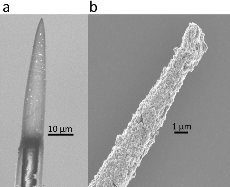
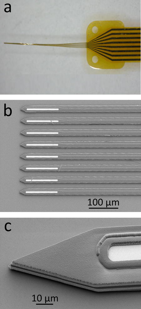
Results: The literature review shows recent efforts to create microelectrodes that are extremely thin appear to reduce or even eliminate the chronic tissue response. With high charge capacity coatings, ultramicroelectrodes fabricated from emerging polymers, and amorphous silicon carbide appear promising for neurostimulation applications.

Conclusion: We envision the emergence of robust and manufacturable ultramicroelectrodes that leverage advanced materials where the small cross-sectional geometry enables compliance within tissue. Nevertheless, future testing under in vivo conditions is particularly important for assessing the stability of thin film devices under chronic stimulation.

Keywords: Coating; deep brain stimulation; electrodes; microelectrode; neural interface; neurostimulation; stimulation.


Conflict of interest statement

Conflict of Interest Statement: The authors have no relevant conflicts of interest to disclose.

Figures

Figure 1
Figure 1
a, An optical micrograph of a commercial, 4×4 cortical microelectrode array produced by Blackrock Microsystems. Using semiconductor processing techniques, a single piece of silicon is fabricated into three dimensional, conical needles. Insulators like Parylene C provide insulation around the individual needles. The conductive tips, consisting of platinum, iridium, or iridium oxide, have a geometric surface area of approximately 2000 μm2; inset shows a scanning electron micrograph of the tip. b, An optical micrograph of an A16 planar Michigan style microelectrode array produced by NeuroNexus. The array is produced in silicon substrates through the addition of multiple conductive and insulating thin films, resulting in an overall device thickness of either 15 or 50 μm. Unlike the Utah style array, the standard singular planar “shank” hosts multiple electrodes, in either linear columns, down the edge of the electrode, or arrayed in sets of four known as tetrodes. The SEM inset shows that limitations from both the planar, two dimensional surface, and real estate lost to route the electrode traces down the shaft of the implant, lead to the NeuroNexus electrodes possessing a smaller geometric surface area of approximately 176 μm2.
Figure 2
Figure 2
Log scale plot comparing Young’s modulus of commonly used implant materials. Implantable electrodes are usually fabricated from high modulus materials such as silicon, which exhibits a modulus 6–7 orders of magnitude higher than that of brain tissue. Softer, polymeric materials such as SU-8 and bio-inspired nanocomposites may decrease this gap by 3–4 orders of magnitude. Values for moduli of each substrate were taken from published literature: Iridium (24), carbon fiber (25,26), platinum (24), silicon (27), a-SiC (28), gold (29), SU-8 (30), Parylene C (31), nanocomposite (32), and human brain tissue (33).
Figure 3
Figure 3
Cartoon depiction of the stiffness of a cantilevered beam subjected to transverse mechanical loads as a representation for a brain implant of length L. I is the moment of inertia, E is the inherent stiffness or modulus of the material, and F is the force required for a deflection, δ.
Figure 4
Figure 4
Bundled 16-channel carbon fiber electrode array. When drawn from water bath, the individual shanks are held by weak van der Waals attraction forming an electrode bundle about 26 μm in diameter (upper right). The fire-sharpened process de-insulates the Parylene C coatings creating an exposed electrode tip whose geometric surface area depends largely on the length of the de-insulated fiber (bottom right). From Guitchounts et al. (26) with permission.
Figure 5
Figure 5
Scanning electron micrograph of a fire-sharpened carbon fiber electrode tip before (left) and after (right) electrodeposited iridium oxide film (EIROF) coatings. EIROF coatings improved the electrochemical properties of the electrode. The nodular surface morphology of EIROF creates a higher electrochemical surface area for charge transfer. With appropriate positive biasing, EIROF coated carbon fiber can readily injected 4 nC/ph in a 200 μs and 400 μs pulses without exceeding water electrolysis limits.
Figure 6
Figure 6
An 8-channel a-SiC microelectrode array (MEA) developed using standard semiconductor fabrication processes. The MEAs are fabricated on a thin layer of polyimide which is spin-coated on a silicon carrier wafer. After fabrication, the carrier wafer is soaked in deionized water to release the devices. a, When withdrawn from deionized water, the shanks of the a-SiC MEA forms a bundle. b, optical micrograph showing the electrode sites at the distal end of the array. Electrode openings are created by reactive ion etching. c, scanning electron micrograph showing the tip profile with a near-vertical sidewall created using an inductively coupled plasma etching system.

References

    1. Benabid AL, Pollak P, Gao DM, Hoffmann D, Limousin P, Gay E, et al. Chronic electrical stimulation of the ventralis intermedius nucleus of the thalamus as a treatment of movement disorders. J Neurosurg. 1996;84:203–214. - PubMed
    1. Flora ED, Perera CL, Cameron AL, Maddern GJ. Deep brain stimulation for essential tremor: A systematic review. Mov Disord. 2010;25:1550–1559. - PubMed
    1. Perlmutter JS, Mink JW. Deep brain stimulation. Annu Rev Neurosci. 2006;29:229–257. - PMC - PubMed
    1. Wichmann T, DeLong MR. Deep brain stimulation for neurologic and neuropsychiatric disorders. Neuron. 2006;52:197–204. - PubMed
    1. Abelson JL, Curtis GC, Sagher O, Albucher RC, Harrigan M, Taylor SF, et al. Deep brain stimulation for refractory obsessive-compulsive disorder. Biol Psychiatry. 2005;57:510–516. - PubMed