. 2017 Nov 24;8(1):1782.
doi: 10.1038/s41467-017-01926-1.

Origami silicon optoelectronics for hemispherical electronic eye systems

Affiliations

Origami silicon optoelectronics for hemispherical electronic eye systems

Kan Zhang et al. Nat Commun. .

Abstract

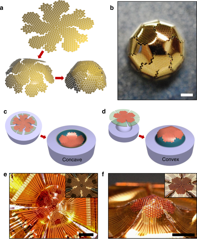
Digital image sensors in hemispherical geometries offer unique imaging advantages over their planar counterparts, such as wide field of view and low aberrations. Deforming miniature semiconductor-based sensors with high-spatial resolution into such format is challenging. Here we report a simple origami approach for fabricating single-crystalline silicon-based focal plane arrays and artificial compound eyes that have hemisphere-like structures. Convex isogonal polyhedral concepts allow certain combinations of polygons to fold into spherical formats. Using each polygon block as a sensor pixel, the silicon-based devices are shaped into maps of truncated icosahedron and fabricated on flexible sheets and further folded either into a concave or convex hemisphere. These two electronic eye prototypes represent simple and low-cost methods as well as flexible optimization parameters in terms of pixel density and design. Results demonstrated in this work combined with miniature size and simplicity of the design establish practical technology for integration with conventional electronic devices.


Conflict of interest statement

The authors declare no competing financial interests.

Figures

Fig. 1
Fig. 1
Geometric origami of silicon optoelectronics for the hemispherical electronic eye. a Schematic illustration of the net of half truncated icosahedron being folded into a hemisphere. 676 polygon blocks consisting of pentagons and hexagons were mapped into a net of subdivided half truncated icosahedron which was then folded to form a hemisphere. b A photograph of the half truncated icosahedron based on polygon blocks of metal-coated silicon nanomembranes printed on a flexible polyimide film. The completed net was folded into a convex hemisphere by inserting the net into a circular hole of a metal fixture. Scale bar, 1 mm. c Schematic illustration of the net of half truncated icosahedron based on silicon nanomembranes pressed into a hemispherical concave mold. d Schematic illustration of the net of half truncated icosahedron based on silicon nanomembranes covered on a hemispherical convex mold. e A photograph of a silicon optoelectronics-based hemispherical focal plane array formed using the concave mold-based origami approach shown in c. Inset image shows the flat focal plane array before folding. Scale bar, 2 mm. f A photograph of a silicon optoelectronics-based convex hemispherical eye camera formed using the convex mold-based origami approach shown in d. Inset image shows the flat eye camera before folding. Scale bar, 2 mm
Fig. 2
Fig. 2
Electrical properties of a silicon optoelectronic device used for the electronic eyes. a Schematic illustration of a hexagon-shaped silicon nanomembrane-based photodiode used for the electronic eyes. An array of such photodiodes were printed and fabricated on a pre-cut flexible polyimide substrate. b Optical microscope image of the photodiodes. Scale bar, 50 μm. c Current density–voltage characteristics of the photodiode in the dark and under the illumination of lasers with wavelengths of 543 (green), 594 (yellow), and 633 nm (red). d Responsivity and external quantum efficiency of the photodiode under the illumination of lasers with green, yellow, and red wavelengths. The laser light intensities were 5 mW for the green and yellow wavelengths and 7 mW for the red wavelength. Green laser was used for the rest of this study
Fig. 3
Fig. 3
A concave hemispherical electronic eye camera system using origami silicon optoelectronics. a Schematic illustration of the hemispherical focal plane array (FPA) based on origami silicon optoelectronics. Fully formed photodiode array fabricated into a net of half truncated icosahedron was pressed and folded into a concave mold to create the hemispherical geometry. b Optics setup of the hemispherical electronic eye system shown using a schematic illustration with a light source, imaged object, and plano-convex lens to the left of the FPA. c A photograph of the hemispherical FPA based on origami silicon optoelectronics. Inset image shows a photograph of the electronic eye system with the plano-convex lens integrated on top of the FPA. Scale bar, 1 mm. d Ray patterns traced from different angles plotted against the position from the object plane. Right inset plot shows a magnified view of the dotted box shown in the plot. Left inset shows the calculated focal plane of the ray passing through the plano-convex lens (dotted red curve) and measured focal plane of the silicon optoelectronics array (blue curve). e High-resolution image of the letter ‘W’ acquired from the hemispherical electronic eye camera. The image was scanned from 0° to 60° in 12° increments for the refined imaging. Each inset image shows a snapshot at each degree angle, with the reference photodiode highlighted in green. f High-resolution image of the letter ‘W’ acquired from the hemispherical electronic eye camera matching the concave hemispherical surface of the FPA
Fig. 4
Fig. 4
A convex hemispherical electronic eye camera system using origami silicon optoelectronics. a Schematic illustration of the convex hemispherical electronic eye camera based on origami silicon optoelectronics. Fully formed photodiode array fabricated into a net of half truncated icosahedron was covered and folded onto a convex mold to create the hemispherical geometry. b A photograph of the convex hemispherical electronic eye camera based on origami silicon optoelectronics. Each photodiode is integrated with a polymer microlens to mimic the corneal lens in a compound eye. Inset image shows a photograph of the compound electronic eye system mounted on a printed circuit board. Scale bar, 1 mm. c Optics setup of the compound electronic eye system shown using a schematic illustration, where the point laser is illuminated from an incident angle of 36°. d Image of the laser point acquired from the compound electronic eye camera matching the convex surface of the camera

References

    1. Lurie-Luke E. Product and technology innovation: What can biomimicry inspire? Biotechnol. Adv. 2014;32:1494–1505. doi: 10.1016/j.biotechadv.2014.10.002. - DOI - PubMed
    1. Raut HK, Ganesh VA, Nair AS, Ramakrishna S. Anti-reflective coatings: a critical, in-depth review. Energ. Environ. Sci. 2011;4:3779–3804. doi: 10.1039/c1ee01297e. - DOI
    1. Viollet S, et al. Hardware architecture and cutting-edge assembly process of a tiny curved compound eye. Sensors. 2014;14:21702–21721. doi: 10.3390/s141121702. - DOI - PMC - PubMed
    1. Atchison, D. A. & Smith, G. in Optics of the Human Eye 3–10 (Butterworth-Heinemann, 2000).
    1. Warrant, E. & Nilsson, D. E. Invertebrate Vision (Cambridge University Press, 2006).

Publication types