. 2017 Dec 5;17(12):2816.
doi: 10.3390/s17122816.

A 45 nm Stacked CMOS Image Sensor Process Technology for Submicron Pixel

Affiliations

A 45 nm Stacked CMOS Image Sensor Process Technology for Submicron Pixel

Seiji Takahashi et al. Sensors (Basel). .

Abstract

A submicron pixel's light and dark performance were studied by experiment and simulation. An advanced node technology incorporated with a stacked CMOS image sensor (CIS) is promising in that it may enhance performance. In this work, we demonstrated a low dark current of 3.2 e-/s at 60 °C, an ultra-low read noise of 0.90 e-·rms, a high full well capacity (FWC) of 4100 e-, and blooming of 0.5% in 0.9 μm pixels with a pixel supply voltage of 2.8 V. In addition, the simulation study result of 0.8 μm pixels is discussed.

Keywords: dark current; full well capacity; image sensor; optical crosstalk; random telegraph noise; read noise; stacked CMOS image sensor; submicron pixel.


Conflict of interest statement

The authors declare no conflict of interest.

Figures

Figure 1
Figure 1
Challenges in submicron pixel generation. (a) Top view of pixel layout highlights the small size source follower; (b) top view of pixel layout indicating the small fill factor; (c) cross-sectional view of pixel depicting high ion implant damage induced by the high dose photodiode; (d) cross-sectional view of pixel showing high optical crosstalk.
Figure 2
Figure 2
Block diagram of 45 nm stacked CIS test vehicle.
Figure 3
Figure 3
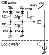
A unit pixel circuit and device partition.
Figure 4
Figure 4
Defects that influence the source follower device noise.
Figure 5
Figure 5
Statistical read noise distributions of the 0.9 μm pixel and the 1.1 μm pixel at an analog gain of 18 dB.
Figure 6
Figure 6
Pixel generation vs. the photodiode implant dose.
Figure 7
Figure 7
Dark current sources marked by “X” and pixel biases.
Figure 8
Figure 8
Schematic drawing of pixel design concept.
Figure 9
Figure 9
Photodiode potential profile. Dashed line is based on control pixel, and solid line is based on the pixel in this experiment.
Figure 10
Figure 10
3D TCAD simulations of the transfer device structure showing electrostatic potential contours. (a) The control pixel during the integration phase; (b) the pixel in this experiment during the integration phase; (c) the control pixel during the read out phase; (d) the pixel in this experiment during the read out phase.
Figure 11
Figure 11
Dark current histograms at 60 °C of the 0.9 μm pixel and the 1.1 μm pixel. The gray color indicates the 1.1 μm pixel, and the black color indicates the 0.9 μm pixel.
Figure 12
Figure 12
Light response curve of the 0.9 μm pixel.
Figure 13
Figure 13
Schematic cross-sectional views of pixel. (a) Control pixel; (b) crosstalk-improved pixel.
Figure 14
Figure 14
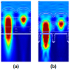
Optical simulation results at an incident wavelength of 530 nm. (a) Control pixel; (b) crosstalk-improved pixel.
Figure 15
Figure 15
Measured quantum efficiency spectra of 0.9 μm pixels. Dashed line is the control 0.9 μm pixel, and the solid line is the improved 0.9 μm pixel.
Figure 16
Figure 16
A sample color image taken with the 0.9 μm pixel manufactured in the 45 nm stacked CIS.
Figure 17
Figure 17
Three-dimensional TCAD simulations of photodiode showing electrostatic potential contours. (a) Two 0.9 μm pixels; (b) two 0.8 μm pixels.

References

    1. Fossum E.R. What to do with sub-diffraction-limit (SDL) pixels?—A proposal for a gigapixel digital film sensor (DFS); Proceedings of the IEEE Workshop on Charge-Coupled Devices and Advanced Image Sensors; Nagano, Japan. 8–11 June 2005; pp. 214–217.
    1. Jung Y.J. Enhancement of low light level images using color-plus-mono dual camera. Opt. Express. 2017;25:12029–12051. doi: 10.1364/OE.25.012029. - DOI - PubMed
    1. Kobayashi M., Johnson M., Wada Y., Tsuboi H., Ono T., Takada H., Togo K., Kishi T., Takahashi H., Ichikawa T., et al. A Low Noise and High Sensitivity Image Sensor with Imaging and Phase-Difference Detection AF in All Pixels. ITE Trans. Media Technol. Appl. 2016;4:123–128. doi: 10.3169/mta.4.123. - DOI
    1. Ahn J.C., Moon C.R., Kim B., Lee K., Kim Y., Lim M., Lee W., Park H., Moon K., Yoo J., et al. Advanced image sensor technology for pixel scaling down toward 1.0 µm (Invited); Proceedings of the IEEE International Electron Devices Meeting; San Francisco, CA, USA. 15–17 December 2008; pp. 1–4.
    1. Wuu S.G., Wang C.C., Hsieh B.C., Tu Y.L., Tseng C.H., Hsu T.H., Hsiao R.S., Takahashi S., Lin R.J., Tsai C.S., et al. A leading-edge 0.9 µm pixel CMOS image sensor technology with backside illumination: Future challenges for pixel scaling; Proceedings of the IEEE International Electron Devices Meeting; San Francisco, CA, USA. 6–8 December 2010.