. 2017 Dec 8;8(1):2014.
doi: 10.1038/s41467-017-02025-x.

Alloy-assisted deposition of three-dimensional arrays of atomic gold catalyst for crystal growth studies

Affiliations

Alloy-assisted deposition of three-dimensional arrays of atomic gold catalyst for crystal growth studies

Yin Fang et al. Nat Commun. .

Abstract

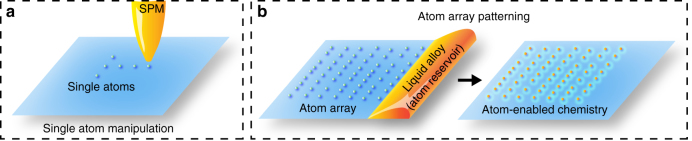
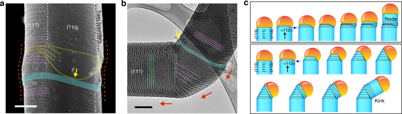
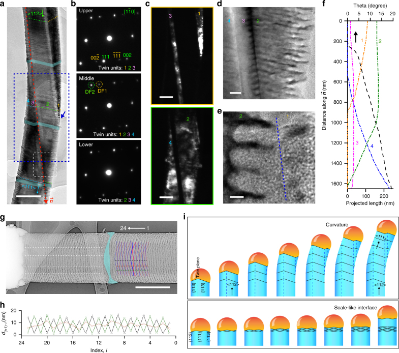
Large-scale assembly of individual atoms over smooth surfaces is difficult to achieve. A configuration of an atom reservoir, in which individual atoms can be readily extracted, may successfully address this challenge. In this work, we demonstrate that a liquid gold-silicon alloy established in classical vapor-liquid-solid growth can deposit ordered and three-dimensional rings of isolated gold atoms over silicon nanowire sidewalls. We perform ab initio molecular dynamics simulation and unveil a surprising single atomic gold-catalyzed chemical etching of silicon. Experimental verification of this catalytic process in silicon nanowires yields dopant-dependent, massive and ordered 3D grooves with spacing down to ~5 nm. Finally, we use these grooves as self-labeled and ex situ markers to resolve several complex silicon growths, including the formation of nodes, kinks, scale-like interfaces, and curved backbones.


Conflict of interest statement

The authors declare no competing financial interests.

Figures

Fig. 1
Fig. 1
Liquid alloy may be used for atom manipulation. a Schematic illustrations of single atom manipulation by SPM and b large-scale and sequential manipulation of atom arrays with liquid alloy
Fig. 2
Fig. 2
Atomic Au lines form over Si nanowire sidewalls. a Schematics of microtomed samples for STEM and FIB-milled samples for APT characterizations, showing the regions of interest. b An aberration-corrected STEM image of ordered line patterns over Si surfaces. Scale bar, 10 nm. c A high-resolution STEM image for a zoom-in view from b (region labeled with blue dashed box). Scale bar, 5 nm. d Isolated gold atoms images highlighted in the line regions from c (marked by two green dashed boxes). Scale bar, 1 nm. e APT analysis displays the 3D atom-by-atom chemical reconstruction of a nanowire surface region. Atomic positions are represented by blue (Si, 2.5% shown), cyan (O, 100% shown), and green (Ni, 10% shown) dots. Scale bar, 20 nm. f A 2D color-coded map of gold atomic density exhibits a chain-like arrangement, indicated by a black dashed arrow. Orange spheres represent gold atoms. Scale bar, 10 nm. g Proximity histogram concentration profile of Si and Au in the direction normal to the Si surface
Fig. 3
Fig. 3
Ab initio molecular dynamics simulation of the catalytic effect of atomic Au. a A representative AIMD snapshot (left) and the corresponding charge transfer between Au and Si atoms (right) at t = 5 ps. Atoms are represented as almond (Si), yellow (Au), red (O), cyan (F), and blue (H) spheres. Isosurfaces represent volumes where electron density decreases (blue) and increases (red) due to the influence of the Au atom. b A histogram showing the distribution of charges on Si atoms bonded to Au (blue) and faraway bulk Si (red) atoms. Si atoms bonded to Au have the highest positive charges. c An AIMD snapshot sampled at a later time point, i.e., t = 41.7 ps. In both sampled configurations, the first nearest-neighbor Si atoms lose electrons to the more electronegative Au atom. This increase in electropositivity of adjacent Si atoms translates to higher reactivity in the presence of electron-rich species such as OH and HF. d Relative height and square displacement (SD) of the Au atom over the course of the simulation. Within the first 10 ps, the surface Au atom moved to the subsurface. An enhanced in-plane mobility was observed in the subsequent 15 ps
Fig. 4
Fig. 4
Atomic Au-catalyzed etching on Si nanowires. a TEM and SEM images showing ordered and 3D grooves over the entire n-type nanowire surfaces. Scale bars, 200 nm. b Schematics of the structure model of gold line patterns and the corresponding etched grooves on Si nanowire sidewall facets. Secondary building units before and after etching are highlighted. A twin plane is usually observed for <112> grown Si nanowires. c Statistical analyses of the groove spacing indicate the effects of the nanowire diameter (n = 36 (blue), 41 (red), and 43 (black)), growth temperature (n = 21 (magenta), 11 (blue), 32 (red), and 11(black)), and Si/P feeding ratio (n = 75 (blue), 92 (red), and 57 (black)) on the groove formation. Boxes, error bars, and dots represent standard errors, standard deviations, and maximum and minimal values, respectively. Dashed and solid lines represent mean and median values, respectively. d, e TEM and SEM images of etched dopant-modulated nanowires. Only the n-type segments yielded the grooves upon etching while the intrinsic segments (cyan ribbons in d, and the middle segment in e) remained smooth. Scale bars, 200 nm (d), 100 nm (e). f Schematic diagrams illustrating the mechanism for atomic Au line pattern formation. A model is proposed, combining a stick-slip motion and a Au deposition process. See Supplementary Discussion (analysis of atomic gold deposition) for details
Fig. 5
Fig. 5
Atomic gold patterns enable the study of the growth dynamics of existing structures. a A SEM image of a nanowire with a node. Yellow and pink dashed lines mark the evolution of the alloy droplet during node formation. The yellow arrow marks the pinning edge of the droplet on an intrinsic segment (cyan ribbon). Red dashed lines highlight the node evolution. Scale bar, 100 nm. b A TEM image of a kinked nanowire. Red arrows indicate the switches of the nanowire growth orientations. The yellow arrow marks the pinning edge of the droplet on the sidewall at an intrinsic segment (cyan ribbon). Pink and green dashed lines highlight the grooves in the original and the new arms, respectively. Scale bar, 100 nm. c Schematics of the growth dynamics. A node is formed when the droplet edge first gets pinned heavily on one facet (blue arrow) while the rest of the droplet continues to evolve. Subsequent unpinning recovers the original growth behavior, leaving a node behind. In the formation of a kinked unit, the pinned droplet edge remains attached to the Si sidewall (blue arrow), while the growth orientation switches between two <112> directions by shrinking/enlarging the Au/Si alloy droplet/Si nanowire interfaces that yield the original/new arm orientations
Fig. 6
Fig. 6
Atomic gold patterns enable the discovery of new crystal growth behaviors. a A BF TEM image of the nanowire with multiple twin units labeled by numbers. The growth orientation is shifted gradually from <112> to <111>. Cyan ribbons highlight the intrinsic segments. Scale bar, 200 nm. b SAED patterns taken at upper, middle, and lower portions of the nanowire in a. c DF TEM images formed by selecting diffraction spots marked by yellow (DF1) and green (DF2) dashed circles in b. Scale bars, 100 nm. d, e HRTEM images from different regions in a, marked by a white dashed box (d) and a blue arrow (e). Scale bars, 20 nm (d), 5 nm (e). f Growth behavior analysis shows a smooth transition of the nanowire orientation from a <112> (marked by n in a) to a <111> direction. Projected lengths of individual twin units and the nanowire angular orientation are plotted along n. g A TEM image (with color inversion) of a nanowire with a scale-like TPB. Scale bar, 200 nm. h The growth behavior is analyzed by tracking spacing d (i+1)–i between adjacent wavy lines (blue and pink lines) at three different locations (black, brown, and green dashed lines in g). The white arrow in g indicates the direction of analysis. i Schematics of the growth dynamics. A curved nanowire can be formed when it gradually switches the growth orientation from <112> to <111> (black arrows), without involving a kink unit. During the transition, the droplet crosses multiple twin boundaries, marked by black dashed lines. A scale-like alloy/Si interface is formed when the TPB oscillates between two wavy line shapes. The cyan ribbon in a and g marks an intrinsic segment

References

    1. Custance O, Perez R, Morita S. Atomic force microscopy as a tool for atom manipulation. Nat. Nanotechnol. 2009;4:803–810. doi: 10.1038/nnano.2009.347. - DOI - PubMed
    1. Eigler DM, Schweizer EK. Positioning single atoms with a scanning tunneling microscope. Nature. 1990;344:524–526. doi: 10.1038/344524a0. - DOI
    1. Hla SW, Rieder KH. STM control of chemical reactions: single-molecule synthesis. Annu. Rev. Phys. Chem. 2003;54:307–330. doi: 10.1146/annurev.physchem.54.011002.103852. - DOI - PubMed
    1. Jung TM, Prokes SM, Kaplan R. Growth and energetics of Ga and Al chains on Si (112) J. Vac. Sci. Technol. A. 1994;12:1838–1842. doi: 10.1116/1.579014. - DOI
    1. Moutanabbir O, et al. Atomically smooth p-doped silicon nanowires catalyzed by aluminum at low temperature. ACS Nano. 2011;5:1313–1320. doi: 10.1021/nn1030274. - DOI - PubMed

Publication types