Review
. 2017 Dec 7:11:665.
doi: 10.3389/fnins.2017.00665. eCollection 2017.

Neural Interfaces for Intracortical Recording: Requirements, Fabrication Methods, and Characteristics

Affiliations
Review

Neural Interfaces for Intracortical Recording: Requirements, Fabrication Methods, and Characteristics

Katarzyna M Szostak et al. Front Neurosci. .

Abstract

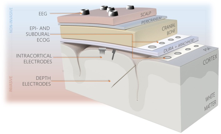
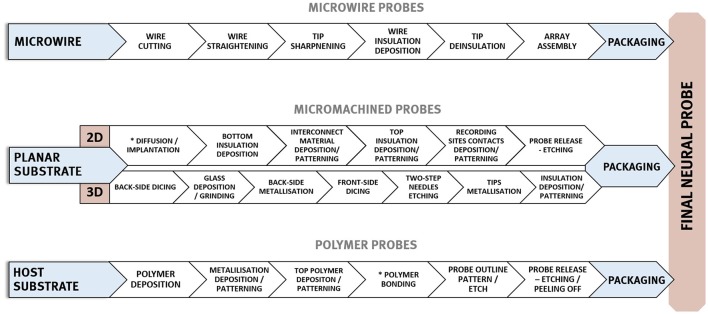
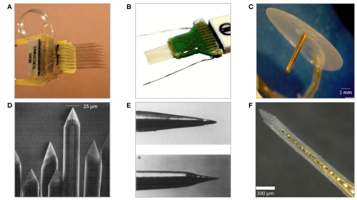
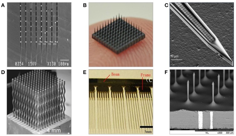
Implantable neural interfaces for central nervous system research have been designed with wire, polymer, or micromachining technologies over the past 70 years. Research on biocompatible materials, ideal probe shapes, and insertion methods has resulted in building more and more capable neural interfaces. Although the trend is promising, the long-term reliability of such devices has not yet met the required criteria for chronic human application. The performance of neural interfaces in chronic settings often degrades due to foreign body response to the implant that is initiated by the surgical procedure, and related to the probe structure, and material properties used in fabricating the neural interface. In this review, we identify the key requirements for neural interfaces for intracortical recording, describe the three different types of probes-microwire, micromachined, and polymer-based probes; their materials, fabrication methods, and discuss their characteristics and related challenges.

Keywords: fabrication; implantable; intracortical; microelectrode; microsystem; neural interface; neural probe.


Figures

Figure 1
Figure 1
Top: Timescale of achievements in brain neuronal recording (Adrian and Bronk, ; Williams and Parsons-Smith, ; Hubel and Wiesel, ; Marg and Adams, ; Halgren et al., ; Georgopoulos et al., ; Ojemann et al., ; Riehle et al., ; Kennedy and Bakay, ; Stanley et al., ; Nicolelis et al., ; Hochberg et al., 2006). Bottom: Timescale of progress in technology of brain-computer interfaces (Rheinberger and Jasper, ; Grundfest et al., ; Jules, ; Wise et al., ; Bak and Salcman, ; Loeb et al., ; Krüger and Bach, ; Najafi et al., ; Campbell et al., ; Laermer and Schilp, ; Cheung et al., ; Rousche et al., ; Cui and Martin, ; Zhong et al., ; Capadona et al., ; Skousen et al., 2015).
Figure 2
Figure 2
Types of brain interfacing electrodes and their location in the reference to the brain. Less invasive systems (blue background) provide recordings of lower resolution in comparison to intracortically-implanted electrodes.
Figure 3
Figure 3
General, exemplary fabrication procedures employed in the formation of three main neural implants' types—micro wire based, micromachined silicon, and micromachined polymer-based probes.
Figure 4
Figure 4
Examples of microwire-based technology neural electrodes (A) 64 channel, floating, discrete 8 × 8 microwire electrode array assembled into connector (Lehew and Nicolelis, 2008). (B) Tucker Davis' 32-channel layered polyimide-insulated tungsten wire array assembled onto custom PCB. (C) Plexon's 24 channel linear Thumbtack microelectrode array (Ulbert et al., 2001). (D) Tips of insulated microwires sharpened mechanically on grinding wheels (Kaltenbach and Gerstein, 1986). (E) Various tips' shapes of eligiloy achieved by electrochemical sharpening of a microwire (Ashford et al., 1985). (F) University's of California 32-channel shank microelectrode array of gold microwires assembled within epoxy shank (Merlo et al., 2012).
Figure 5
Figure 5
Examples of neural microelectrodes fabricated with micromachining methods on silicon substrate. (A) Michigan electrode—style 64-channel planar probes defined mainly with photolithography (Kindlundh et al., 2004). (B) 10 × 10 Utah electrode array fabricated from thick substrates by dicing and etching, size of array is roughly 4 × 4 mm (Yoo et al., 2012). (C) 1000-channel close-packed silicon microelectrode fabricated combining electron beam and standard photolithography (Scholvin et al., 2016). (D) Multineedle electrode array fabricated with wire electron discharge machining allowing for non 3D needle-shaping (Rakwal et al., 2009). (E) All-silicon wire electrodes fabricated by combination of wet and dry etching processes (Pei et al., 2014). (F) TSV-integrated silicon microneedle array (Chang et al., 2015).
Figure 6
Figure 6
Neural microelectrodes fabricated from various materials with the use of micromachining methods (A) Three-dimensional, flexible macroporous thin layer metal microelectrode (Xie et al., 2015) (B) Highly flexible metal layer electrodes with implantation-enabling dissolvable gelatine matrix (Agorelius et al., 2015) (C) Diamond-based planar microelectrode (Chan et al., 2009) (D) Ceramic-based planar microelectrode (Burmeister et al., 2000) (E) Multilayer planar glass-based microelectrodes array (Lee et al., 2009) (F) Three-dimensional, aluminum-based 6 × 6 multineedle metal microelectrode (Goncalves et al., 2014).
Figure 7
Figure 7
Polymer-based neural microelectrodes formed with a use of microfabrication techniques and host substrates. (A) Flexible polyimide-based planar multisite shank electrode (Mercanzini et al., 2008). (B) Parylene-C/SU-8-based flexible microelectrode with thin lateral arms allowing for mechanical mismatch compensation (Seymour and Kipke, 2006). (C) Polyimide-based fishbone-shaped microelectrode (Wu et al., 2011). (D) Polyimide-based three dimensional multichannel electrode (Takeuchi et al., 2003). (E) Three-dimensional thermoformed Parylene-C-based cone polymer sheath electrode (Kuo et al., 2013). (F) Parylene-C-based sinusoidal electrode (Sohal et al., 2014).

References

    1. Aarts A. A. A., Srivannavit O., Wise K. D., Yoon E., Puers R., Van Hoof C., et al. (2011). Fabrication technique of a compressible biocompatible interconnect using a thin film transfer process. J. Micromech. Microeng. 21:074012 10.1088/0960-1317/21/7/074012 - DOI
    1. Adamov M., Perović B., Nenadović T. (1974). Electrical and structural properties of thin gold films obtained by vacuum evaporation and sputtering. Thin Solid Films 24, 89–100. 10.1016/0040-6090(74)90254-5 - DOI
    1. Adrian E. D., Bronk D. W. (1929). The discharge of impulses in motor nerve fibres. J. Physiol. 67, 9–151. 10.1113/jphysiol.1929.sp002557 - DOI - PMC - PubMed
    1. Agorelius J., Tsanakalis F., Friberg A., Thorbergsson P. T., Pettersson L. M., Schouenborg J. (2015). An array of highly flexible electrodes with a tailored configuration locked by gelatin during implantation—initial evaluation in cortex cerebri of awake rats. Front Neurosci. 9:331. 10.3389/fnins.2015.00331 - DOI - PMC - PubMed
    1. Ashford J. W., Coburn K. L., Fuster J. M. (1985). The elgiloy microelectrode: fabrication techniques and characteristics. J. Neurosci. Methods 14, 247–252. 10.1016/0165-0270(85)90086-X - DOI - PubMed