. 2018 Jan 30;18(3):496-504.
doi: 10.1039/c7lc01052d.

Fundamentals of rapid injection molding for microfluidic cell-based assays

Affiliations

Fundamentals of rapid injection molding for microfluidic cell-based assays

Ulri N Lee et al. Lab Chip. .

Abstract

Microscale cell-based assays have demonstrated unique capabilities in reproducing important cellular behaviors for diagnostics and basic biological research. As these assays move beyond the prototyping stage and into biological and clinical research environments, there is a need to produce microscale culture platforms more rapidly, cost-effectively, and reproducibly. 'Rapid' injection molding is poised to meet this need as it enables some of the benefits of traditional high volume injection molding at a fraction of the cost. However, rapid injection molding has limitations due to the material and methods used for mold fabrication. Here, we characterize advantages and limitations of rapid injection molding for microfluidic device fabrication through measurement of key features for cell culture applications including channel geometry, feature consistency, floor thickness, and surface polishing. We demonstrate phase contrast and fluorescence imaging of cells grown in rapid injection molded devices and provide design recommendations to successfully utilize rapid injection molding methods for microscale cell-based assay development in academic laboratory settings.


Conflict of interest statement

§ The authors acknowledge the following potential conflicts of interest: EB: Tasso, Inc., Salus Discovery, LLC and Stacks to the Future, LLC, DJG: Salus Discovery, LLC and Tasso, Inc., ABT: Stacks to the Future, LLC.

Figures
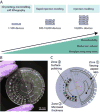
Figure 1
Figure 1
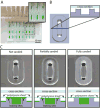
(A) Microscale device fabrication methods compared for their advantages and limitations. (B) Photograph of the PS device designed to test key characteristics of rapid injection molding for microscale cell-based applications. Photos of PP and COC test devices are shown in Figure S1. (C) Schematic of test device highlighting features of interest designed to test key requirements for microscale cell-based applications including rectangular channels positioned parallel and perpendicular to the plastic flow (zone 1), microwells for phase contrast microscopy (zone 2), and microwells for fluorescence microscopy (zone 3).
Figure 2
Figure 2
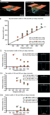
Quantification of dimensional differences between the device design and the injection molded device (PS device only). (A) Confocal microscope images of channels (designed width = 300 μm; left channel designed height = 150 μm, right channel designed height = 500 μm). The blue line indicates the cross section used for dimension measurements. Measurements of width were made at both the top and the bottom of the channel. (B) Comparison between the average measured width and the designed width for the 150 μm and 500 μm deep channels (the y=x line, representing ideal correspondence between designed and measured values). (Ci-Ciii) Plots of relative deviation for the parameters indicated (left) and corresponding confocal profilometer cross-sections (right). Data points represent the average of three devices produced by the same mold. In all cases, the standard error of the mean was smaller than the symbol plotted; the complete set of raw data is included in the SI, including separately plotted data points for the three replicate devices.
Figure 3
Figure 3
Effect of feature orientation relative to the flow of plastic in the mold for PS devices. (A) Schematic of molten plastic flow around mold for channels perpendicular (top) and parallel (bottom) to the flow of plastic. (Flow of plastic in the schematic is represented by light blue shading and arrows.) (B) Graph of average relative deviation in top width for rectangular channels parallel and perpendicular to the PS flow. Data points represent the average of three devices produced by the same mold. In cases where the standard error of the mean was smaller than the symbols plotted, error bars are not shown; the complete set of raw data is included in the SI, including separately plotted data points for the three replicate devices.
Figure 4
Figure 4
Effect of aluminium mold polishing on surface roughness of COC microwells and on clarity of phase contrast microscopy images of cells grown in COC microwells. The results indicate that the highest level of polishing (SPI_A2) is required for clear phase contrast images. Microwells corresponding to the data presented in this figure are shown in zone 2 of the test device schematic (Figure 1C), with the same color-coding to represent the level of polishing applied to the metal mold. Abbreviations “PM_F0” though “SPI_A2” correspond to the polishing level options offered by Proto Labs® (see further explanation in Results section). (A) Top row: Optical microscopy images of COC microwells without cells imaged using a 3D laser scanning confocal microscope. Bottom row: Phase contrast microscopy images (10× magnification) of prostate epithelial cells (BHPrE1) grown on COC microwells; original images are included in Figure S9. Images are representative of two replicate microwells from one device. (B) Surface roughness (root mean squared (RMS) height) of COC surfaces measured using 3D laser scanning confocal microscopy. The bars indicate the mean of two replicate microwells from one device (data points from two replicates are superimposed on the bars).
Figure 5
Figure 5
Fluorescence microscopy images of cells grown in COC microwells of varied thickness and polishing. Fluorescence images of prostate epithelial cells (BHPrE1) taken at 20× (0,40 NA) magnification with nuclear staining (DAPI, blue), proliferating nuclei (EdU, red), and tubulin (green). Zoomed in images of areas outlined in white are on the bottom row. The original images (with larger field of view) are included in Figure S7. The results indicate that the highest polishing level, SPI_A2, and a designed thickness of 100 μm enables clear images. Microwells corresponding to the data presented in this figure are shown in zone 3 of the test device schematic (Fig. 1C). The designed thickness is indicated in this figure; measurements of actual thickness are included in the SI, Figure S6A. Images bordered with red frames correspond to SPI_A2 polishing; green frames correspond to SPI_B1 polishing.
Figure 6
Figure 6
Closed channel cell culture device fabricated by solvent bonding a PS sheet (comprising the channel floor) and a PS injection molded device (comprising the channel walls and ceiling). (A) Closed channel cell culture device with multiplexed channel filling using a multichannel pipette. (B) Schematic of a single channel with oval island surrounding the channel. The cross-section (inset) shows that the oval island surrounding the channel is slightly curved due to plastic sinking caused by variable cooling rates of thick and thin regions of the injection molded device. (C) Schematic diagrams illustrating channel cross sections after solvent bonding to a PS sheet. For clarity the orientation of the schematic matches the orientation of the photographs directly above; when in operation, the device is flipped over such that the PS sheet forms the floor (as shown in A). The schematic diagrams indicate the results of filling the solvent bonded devices with fluid (green); leaking occurs when devices are assembled without sanding. Sanding provides a flat surface for solvent bonding enabling a leak-free device. Photographs show whitened areas of plastic removed by sanding the oval islands.

Similar articles

Cited by

References

    1. Bhatia SN, Ingber DE. Nat Biotechnol. 2014;32:760–772. - PubMed
    1. Kovarik ML, Gach PC, Ornoff DM, Wang Y, Balowski J, Farrag L, Allbritton NL. Anal Chem. 2012;84:516–40. - PMC - PubMed
    1. Huh D, Torisawa YS, Hamilton GA, Kim HJ, Ingber DE. Lab Chip. 2012;12:2156–2164. - PubMed
    1. Sackmann EK, Fulton AL, Beebe DJ. Nature. 2014;507:181–189. - PubMed
    1. An F, Qu Y, Liu X, Zhong R, Luo Y. Anal Chem Insights. 2015;10:39. - PMC - PubMed

Publication types