

DNA multi-bit non-volatile memory and bit-shifting operations using addressable electrode arrays and electric field-induced hybridization
- PMID: 29348493
- PMCID: PMC5773625
- DOI: 10.1038/s41467-017-02705-8
DNA multi-bit non-volatile memory and bit-shifting operations using addressable electrode arrays and electric field-induced hybridization
Abstract
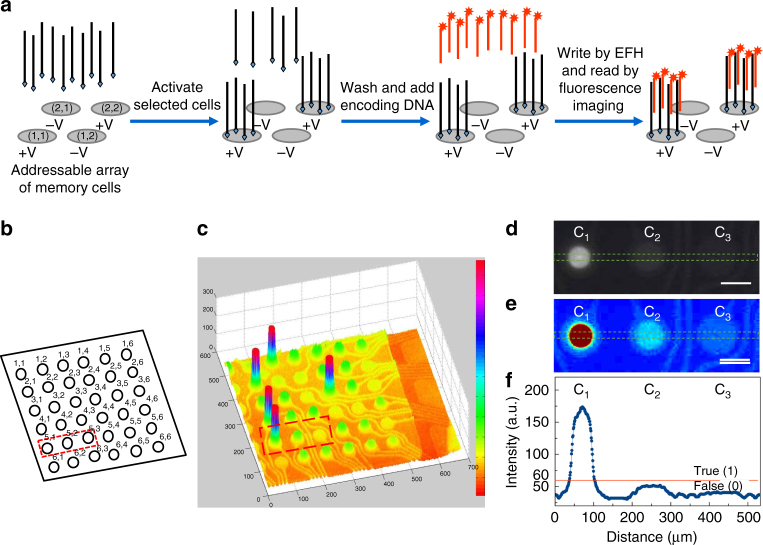
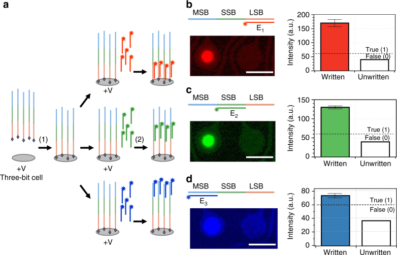
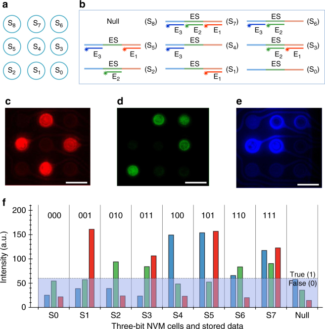
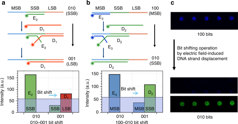
DNA has been employed to either store digital information or to perform parallel molecular computing. Relatively unexplored is the ability to combine DNA-based memory and logical operations in a single platform. Here, we show a DNA tri-level cell non-volatile memory system capable of parallel random-access writing of memory and bit shifting operations. A microchip with an array of individually addressable electrodes was employed to enable random access of the memory cells using electric fields. Three segments on a DNA template molecule were used to encode three data bits. Rapid writing of data bits was enabled by electric field-induced hybridization of fluorescently labeled complementary probes and the data bits were read by fluorescence imaging. We demonstrated the rapid parallel writing and reading of 8 (23) combinations of 3-bit memory data and bit shifting operations by electric field-induced strand displacement. Our system may find potential applications in DNA-based memory and computations.
Conflict of interest statement
The authors declare no competing financial interests.
Figures
Similar articles
-
Multi-bit biomemory consisting of recombinant protein variants, azurin.Biosens Bioelectron. 2009 Jan 1;24(5):1503-7. doi: 10.1016/j.bios.2008.07.080. Epub 2008 Aug 19. Biosens Bioelectron. 2009. PMID: 18809307
-
Electronic microarrays in DNA computing.J Nanosci Nanotechnol. 2011 Mar;11(3):1859-65. doi: 10.1166/jnn.2011.3422. J Nanosci Nanotechnol. 2011. PMID: 21449321
-
Addressable configurations of DNA nanostructures for rewritable memory.Nucleic Acids Res. 2017 Nov 2;45(19):11459-11465. doi: 10.1093/nar/gkx777. Nucleic Acids Res. 2017. PMID: 28977499 Free PMC article.
-
Nucleic Acid Databases and Molecular-Scale Computing.ACS Nano. 2019 Jun 25;13(6):6256-6268. doi: 10.1021/acsnano.9b02562. Epub 2019 May 24. ACS Nano. 2019. PMID: 31117381 Review.
-
DNA as a universal chemical substrate for computing and data storage.Nat Rev Chem. 2024 Mar;8(3):179-194. doi: 10.1038/s41570-024-00576-4. Epub 2024 Feb 9. Nat Rev Chem. 2024. PMID: 38337008 Review.
Cited by
-
A last-in first-out stack data structure implemented in DNA.Nat Commun. 2021 Aug 11;12(1):4861. doi: 10.1038/s41467-021-25023-6. Nat Commun. 2021. PMID: 34381035 Free PMC article.
-
Low cost DNA data storage using photolithographic synthesis and advanced information reconstruction and error correction.Nat Commun. 2020 Oct 22;11(1):5345. doi: 10.1038/s41467-020-19148-3. Nat Commun. 2020. PMID: 33093494 Free PMC article.
-
Processing DNA Storage through Programmable Assembly in a Droplet-Based Fluidics System.Adv Sci (Weinh). 2023 Nov;10(32):e2303197. doi: 10.1002/advs.202303197. Epub 2023 Sep 26. Adv Sci (Weinh). 2023. PMID: 37755129 Free PMC article.
-
Electrochemical DNA synthesis and sequencing on a single electrode with scalability for integrated data storage.Sci Adv. 2021 Nov 12;7(46):eabk0100. doi: 10.1126/sciadv.abk0100. Epub 2021 Nov 12. Sci Adv. 2021. PMID: 34767438 Free PMC article.
-
Uncertainties in synthetic DNA-based data storage.Nucleic Acids Res. 2021 Jun 4;49(10):5451-5469. doi: 10.1093/nar/gkab230. Nucleic Acids Res. 2021. PMID: 33836076 Free PMC article. Review.
References
Publication types
MeSH terms
Substances
Grants and funding
LinkOut - more resources
Full Text Sources
Other Literature Sources
