

3D printed high density, reversible, chip-to-chip microfluidic interconnects
- PMID: 29355276
- PMCID: PMC5811381
- DOI: 10.1039/c7lc01113j
3D printed high density, reversible, chip-to-chip microfluidic interconnects
Abstract
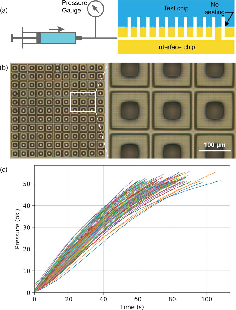
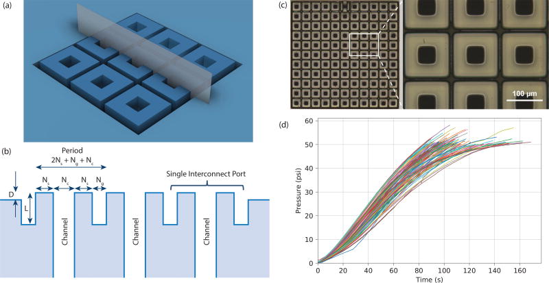
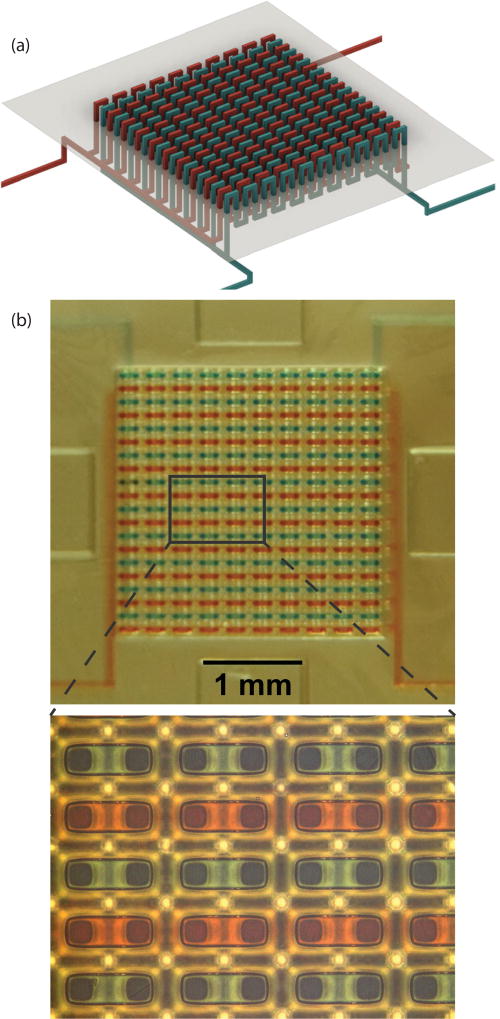
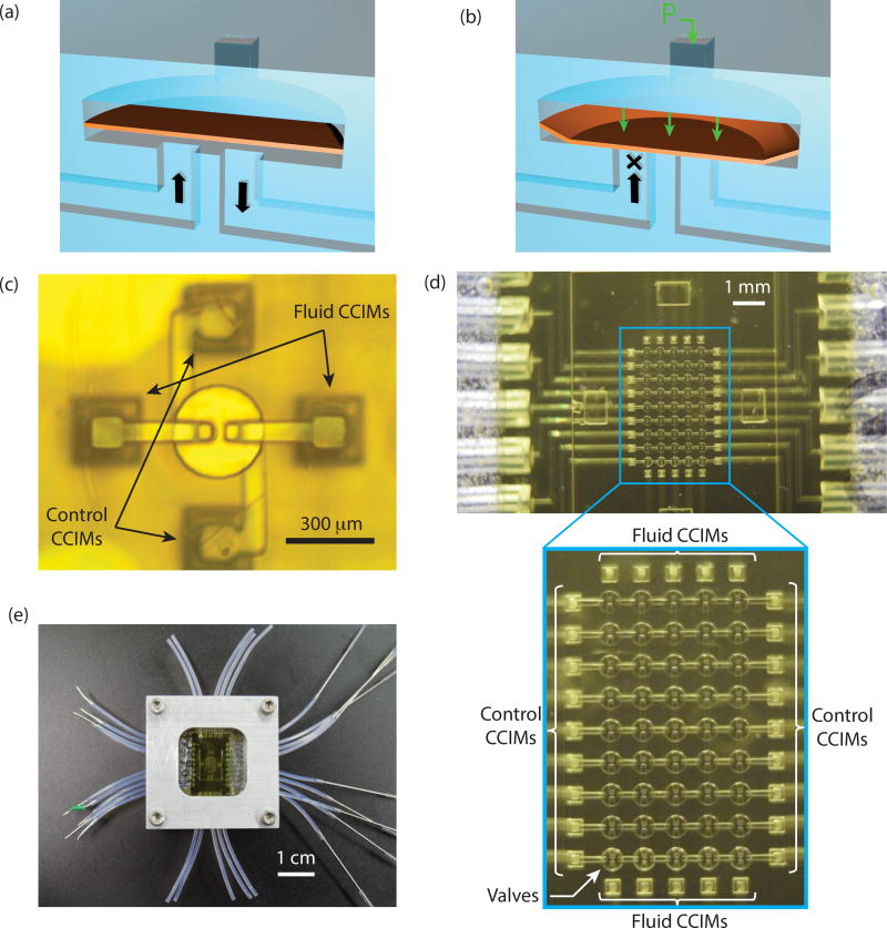
Our latest developments in miniaturizing 3D printed microfluidics [Gong et al., Lab Chip, 2016, 16, 2450; Gong et al., Lab Chip, 2017, 17, 2899] offer the opportunity to fabricate highly integrated chips that measure only a few mm on a side. For such small chips, an interconnection method is needed to provide the necessary world-to-chip reagent and pneumatic connections. In this paper, we introduce simple integrated microgaskets (SIMs) and controlled-compression integrated microgaskets (CCIMs) to connect a small device chip to a larger interface chip that implements world-to-chip connections. SIMs or CCIMs are directly 3D printed as part of the device chip, and therefore no additional materials or components are required to make the connection to the larger 3D printed interface chip. We demonstrate 121 chip-to-chip interconnections in an 11 × 11 array for both SIMs and CCIMs with an areal density of 53 interconnections per mm2 and show that they withstand fluid pressures of 50 psi. We further demonstrate their reusability by testing the devices 100 times without seal failure. Scaling experiments show that 20 × 20 interconnection arrays are feasible and that the CCIM areal density can be increased to 88 interconnections per mm2. We then show the utility of spatially distributed discrete CCIMs by using an interconnection chip with 28 chip-to-world interconnects to test 45 3D printed valves in a 9 × 5 array. Each valve is only 300 μm in diameter (the smallest yet reported for 3D printed valves). Every row of 5 valves is tested to at least 10 000 actuations, with one row tested to 1 000 000 actuations. In all cases, there is no sign of valve failure, and the CCIM interconnections prove an effective means of using a single interface chip to test a series of valve array chips.
Conflict of interest statement
There are no conflicts of interest to declare.
Figures
Similar articles
-
High density 3D printed microfluidic valves, pumps, and multiplexers.Lab Chip. 2016 Jul 7;16(13):2450-8. doi: 10.1039/c6lc00565a. Epub 2016 May 31. Lab Chip. 2016. PMID: 27242064 Free PMC article.
-
Microfluidic Lab-on-CMOS Packaging Using Wafer-Level Molding and 3D-Printed Interconnects.IEEE Trans Biomed Circuits Syst. 2024 Aug;18(4):821-833. doi: 10.1109/TBCAS.2024.3419804. IEEE Trans Biomed Circuits Syst. 2024. PMID: 39167525
-
Modeling of misalignment effects in microfluidic interconnects for modular bio-analytical chip applications.Electrophoresis. 2013 Nov;34(20-21):2988-95. doi: 10.1002/elps.201300110. Epub 2013 Oct 9. Electrophoresis. 2013. PMID: 23893860 Free PMC article.
-
3D printed microfluidics for biological applications.Lab Chip. 2015;15(18):3627-37. doi: 10.1039/c5lc00685f. Lab Chip. 2015. PMID: 26237523 Review.
-
Next-generation integrated microfluidic circuits.Lab Chip. 2011 Sep 7;11(17):2813-8. doi: 10.1039/c1lc20387h. Epub 2011 Jul 28. Lab Chip. 2011. PMID: 21799977 Review.
Cited by
-
Microfluidics: Innovations in Materials and Their Fabrication and Functionalization.Anal Chem. 2020 Jan 7;92(1):150-168. doi: 10.1021/acs.analchem.9b04986. Epub 2019 Dec 2. Anal Chem. 2020. PMID: 31721565 Free PMC article. Review.
-
A compact LED-based projection microstereolithography for producing 3D microstructures.Sci Rep. 2019 Dec 23;9(1):19692. doi: 10.1038/s41598-019-56044-3. Sci Rep. 2019. PMID: 31873101 Free PMC article.
-
3D Printed Microfluidic Devices for Microchip Electrophoresis of Preterm Birth Biomarkers.Anal Chem. 2019 Jun 4;91(11):7418-7425. doi: 10.1021/acs.analchem.9b01395. Epub 2019 May 14. Anal Chem. 2019. PMID: 31056901 Free PMC article.
-
Current and Emerging Technologies for the Detection of Norovirus from Shellfish.Foods. 2019 May 31;8(6):187. doi: 10.3390/foods8060187. Foods. 2019. PMID: 31159220 Free PMC article.
-
[Research advances of high-throughput cell-based drug screening systems based on microfluidic technique].Se Pu. 2021 Jun;39(6):567-577. doi: 10.3724/SP.J.1123.2020.07014. Se Pu. 2021. PMID: 34227317 Free PMC article. Review. Chinese.
References
-
- Bhagat AAS, Jothimuthu P, Pais A, Papautsky I. Journal of Micromechanics and Microengineering. 2006;17:42.
Publication types
MeSH terms
Grants and funding
LinkOut - more resources
Full Text Sources
Other Literature Sources
Miscellaneous