. 2018 Mar;17(3):268-276.
doi: 10.1038/s41563-017-0011-3. Epub 2018 Jan 29.

Morphable 3D mesostructures and microelectronic devices by multistable buckling mechanics

Affiliations

Morphable 3D mesostructures and microelectronic devices by multistable buckling mechanics

Haoran Fu et al. Nat Mater. 2018 Mar.

Abstract

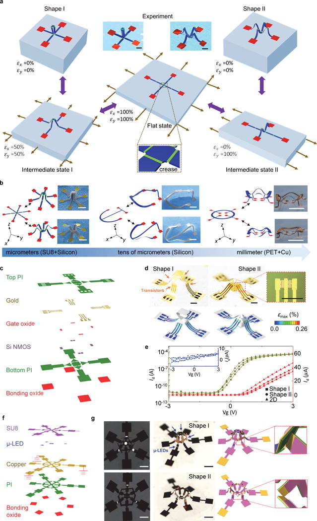
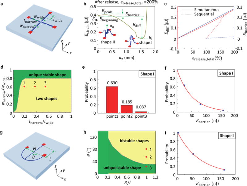
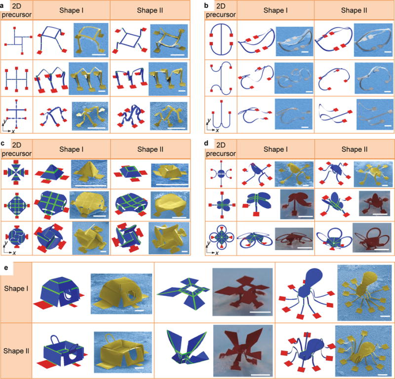
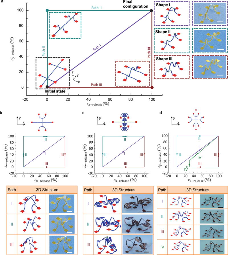
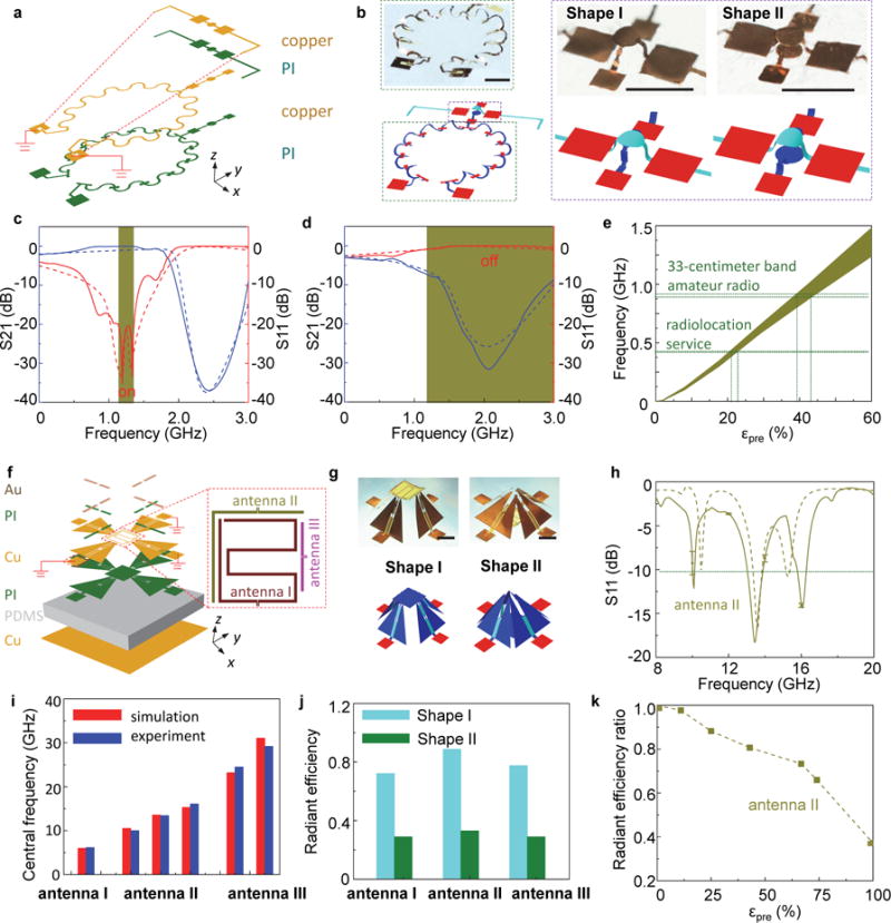
Three-dimensional (3D) structures capable of reversible transformations in their geometrical layouts have important applications across a broad range of areas. Most morphable 3D systems rely on concepts inspired by origami/kirigami or techniques of 3D printing with responsive materials. The development of schemes that can simultaneously apply across a wide range of size scales and with classes of advanced materials found in state-of-the-art microsystem technologies remains challenging. Here, we introduce a set of concepts for morphable 3D mesostructures in diverse materials and fully formed planar devices spanning length scales from micrometres to millimetres. The approaches rely on elastomer platforms deformed in different time sequences to elastically alter the 3D geometries of supported mesostructures via nonlinear mechanical buckling. Over 20 examples have been experimentally and theoretically investigated, including mesostructures that can be reshaped between different geometries as well as those that can morph into three or more distinct states. An adaptive radiofrequency circuit and a concealable electromagnetic device provide examples of functionally reconfigurable microelectronic devices.


Conflict of interest statement

Competing financial interests

The authors declare no competing financial interests.

Figures

Figure 1
Figure 1. Morphable 3D mesostructures and integrated circuits by loading-path controlled mechanical assembly
a, Conceptual illustration of the strategy through a sequence of FEA results and a pair of colorized SEM images of two 3D mesostructures. b, 2D shapes, FEA predictions and corresponding experimental images (SEM or optical) of morphable 3D mesostructures with diverse materials and length scales [left: bilayers of SU8 (1 μm at the creases and 2 μm at the other regions) and Si (50 nm); middle: Si (1.5 μm); right: bilayers of PET (50  μm) and Cu (1  μm)]. Shape I (upper frames) corresponds to simultaneous release and Shape II (lower frames) corresponds to sequential release (y direction first, and then x direction). Scale bars, 50 μm for the left panel; 500 μm for the middle panel; and 5 mm for the right panel. c-e, Design of a morphable 3D structure that embeds several silicon transistors, along with metal interconnects. c, The exploded view of the 2D geometry. d, Optical images of two configurations of the structure after 3D assembly. Shape I and Shape II correspond to simultaneous and sequential release, respectively. Scale bars, 200 μm. e, Current-voltage (I-V) characteristics of a transistor measured with the structure in Shape I, Shape II and the planar state. The color in the FEA results of d corresponds to the magnitude of maximum principal strain in the metal. f and g, Design for a morphable 3D optoelectronic device that incorporates four μ-LEDs. The left shows an exploded view of the 2D geometry, and the right shows optical images and modeling results for two device configurations (Shape I and II). Scale bars, 1 mm.
Figure 2
Figure 2. Probabilistic energy analysis and design rationale for morphable 3D mesostructures
a-f, Analysis for a structure based on a straight ribbon. a, Schematic illustration of a straight ribbon structure. b, Strain energy as a function of out-of-plane displacement for ( lwide,lnarrow,wwide,wnarrow,t, εpre) = (0.77 mm, 0.1 mm, 0.16 mm, 40 μm, 6 μm, 100%) and an elastic modulus of 4.02 GPa. The insets show the stable configurations at the corresponding out-of-plane displacement. Here, l, w and t are the length, width and thickness of the two constituent ribbons, respectively, and the subscripts ‘narrow’ and ‘wide’ denote the creases and other regions, respectively. c, Energy difference and energy barrier versus total release strain for 3D structures that arise from simultaneous and sequential releases. d, Design diagram in the space of length ratio and width ratio. e, Experimentally determined probability for achieving Shape I by sequential release for three different parameter combinations (wnarrow/wwide, lnarrow/lwide)=(0.3,0.2), (0.3,0.4) and (0.3,0.6). f, Dependence of the probability on the magnitude of the energy barrier. g-i, Analysis for the hybrid straight/curved ribbon structure. g, Schematic illustration of a hybrid straight/curved ribbon structure. h, Design diagram in the space of length ratio and arc angle. i, Dependence of the probability on the magnitude of the energy barrier.
Figure 3
Figure 3. A broad set of 3D mesostructures morphable by loading path strategies
a-d, 2D geometries, FEA predictions and experimental images (SEM or optical) of morphable ribbon-shaped mesostructures with and without creases, membrane-shaped mesostructures, and hybrid ribbon/membrane mesostructures. Path I corresponds to simultaneous release, and Path II corresponds to sequential release (y direction first, and then x direction). e, FEA predictions and experimental images (SEM or optical) of morphable, recognizable objects. Certain parts of the structures are not shown in the FEA results for the second and third examples to improve the visibility of the key regions. The complete deformed configurations based on FEA can be found in Supplementary Fig. 10. In all colorized SEM and optical images, the yellow, silver and red colors correspond to SU8 (6 μm for normal region and 2 μm for crease), silicon ( 1.5μm) and PET (40  μm), respectively. Scale bars, 400  μm for samples with SU8 and silicon, and 4 mm for samples with PET.
Figure 4
Figure 4. Morphable 3D mesostructures with multiple ( 3) stable states accessed through complex paths of sequential release
a-d, 2D geometries, release sequences, FEA predictions and experimental images (SEM or optical) of four complex ribbon networks. The yellow and dark brown colors in the colorized experimental images correspond to SU8 (6  μm for normal region and 2  μm for crease), and bilayer of PET (50  μm) and copper (1  μm), respectively. Scale bars, 400  μm for SU8 mesostructures (Fig. 4a-b), and 4 mm for PET/Cu mesostructures (Fig. 4c-d).
Figure 5
Figure 5. Applications of 3D morphable mesostructures as switchable radio frequency (RF) electronic components
a-e, A morphable RF circuit. a, Exploded view illustration of the layer construction [Cu (3  μm), PI (2 μm)]. b, FEA predictions and optical images of the overall device, and magnified view of the capacitor structure that results from different release sequences. Shape I and II result from simultaneous and sequential release (x direction first, and then y) of the elastomer substrate, respectively. Scale bars, 1 mm. c, Measured and simulated S21 and S11 versus frequency for Shape I, when the device is formed from a biaxial prestrain (εx-pre = εy-pre = 60%). d, Measured and simulated S21 and S11 versus frequency for Shape II, when the device is formed from a biaxial prestrain (εx-pre = εy-pre = 60%). e, Simulated switchable frequency band as a function of the prestrain, when the device is subject to different biaxial prestrains. f-i, A morphable electromagnetic device with shielding capability. f, Exploded view of the layer construction [thickness of each layer from top to bottom: Au (100 nm), PI (1.5 μm), Cu (9  μm), PI (12 μm), PDMS (5 mm), Cu (100 nm)]. g, FEA prediction (lower frames) and optical images (upper frames) of the device. Scale bars, 5 mm. h, Measured and simulated dependence of the return loss (S11) on the frequency for antenna II. i, FEA predictions and experimental measurements of the central frequency for antenna I, II and III. j, Simulated radiant efficiency for antenna I (at frequency f=6.0 GHz), II (f=13.58 GHz) and III (f=23.2 GHz) when the device is released from a biaxial prestrain (εx-pre = εy-pre = 85%). k, Simulated radiant efficiency ratio for antenna I (f=6.0 GHz) as a function of the prestrain. In c, d and h, the solid and dash lines correspond to the experiment and simulation results, respectively.

References

    1. Miura K. Method of packaging and deployment of large membranes in space. The Institute of Space and Astronautical Science Report. 1985;618:1.
    1. Kuribayashi-Shigetomi K, Onoe H, Takeuchi S. Cell Origami: Self-Folding of Three-Dimensional Cell-Laden Microstructures Driven by Cell Traction Force. Plos One. 2012;7 - PMC - PubMed
    1. Randall CL, Gultepe E, Gracias DH. Self-folding devices and materials for biomedical applications. Trends Biotechnol. 2012;30:138. - PMC - PubMed
    1. Bishop D, Pardo F, Bolle C, Giles R, Aksyuk V. Silicon Micro-Machines for Fun and Profit. J Low Temp Phys. 2012;169:386.
    1. Felton S, Tolley M, Demaine E, Rus D, Wood R. A method for building self-folding machines. Science. 2014;345:644. - PubMed

Publication types