

Steep switching devices for low power applications: negative differential capacitance/resistance field effect transistors
- PMID: 29399434
- PMCID: PMC5787217
- DOI: 10.1186/s40580-018-0135-4
Steep switching devices for low power applications: negative differential capacitance/resistance field effect transistors
Abstract
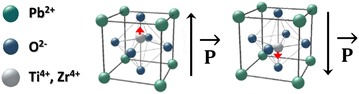
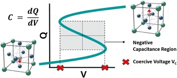
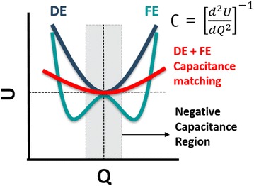
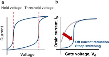
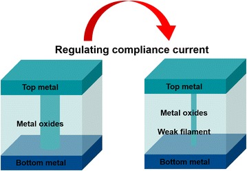
Simply including either single ferroelectric oxide layer or threshold selector, we can make conventional field effect transistor to have super steep switching characteristic, i.e., sub-60-mV/decade of subthreshold slope. One of the representative is negative capacitance FET (NCFET), in which a ferroelectric layer is added within its gate stack. The other is phase FET (i.e., negative resistance FET), in which a threshold selector is added to an electrode (e.g., source or drain) of conventional field effect transistor. Although the concept of the aforementioned two devices was presented more or less recently, numerous studies have been published. In this review paper, by reviewing the published studies over the last decade, we shall de-brief and discuss the history and the future perspectives of NCFET/phase FET, respectively. The background, experimental investigation, and future direction for developing the aforementioned two representative steep switching devices (i.e., NCFET and phase FET/negative resistance FET) are to be discussed in detail.
Keywords: Field effect transistor; Low power application; Negative capacitance; Phase FET; Steep switching device.
Figures
References
-
- Moore GE. Electronics. 1965;38:114–117.
-
- C. Auth, A. Aliyarukunju, M. Asoro, D. Bergstrom, V. Bhagwat, J. Birdsall, N. Bisnik, M. Buehler, V. Chikarmane, G. Ding, Q. Fu, H. Gomez, W. Han, D. Hanken, M. Haran, M. Hattendorf, R. Heussner, H. Hiramatsu, B. Ho, S. Jaloviar, I. Jin, S. Joshi, S. Kirby, S. Kosaraju, H. Kothari, G. Leatherman, K. Lee, J. Leib, A. Madhavan, K. Marla, H. Meyer, T. Mule, C. Parker, S. Parthasarathy, C. Pelto, L. Pipes, I. Post, M. Prince, A. Rahman, S. Rajamani, A. Saha, J.D. Santos, M. Sharma, V. Sharma, J. Shin, P. Shinha, P. Smith, M. Sprinkle, A.S. Amour, C. Staus, R. Suri, D. Towner, A. Tripathi, A. Tura, C. Ward, A. Yeoh, In: Proc. IEEE IEDM 29.1(2017)
-
- Choi WY, Park BG, Lee JD, Liu TJK. IEEE Electron Dev. Lett. 2007;28:743–745. doi: 10.1109/LED.2007.901273. - DOI
-
- Ko E, Lee H, Park JD, Shin C. IEEE Trans. Elect. Dev. 2016;63:5030–5035. doi: 10.1109/TED.2016.2619372. - DOI
-
- Liu TJK, Markovic D, Stojanovic V, Alon E. IEEE Spectr. 2012;49:40. doi: 10.1109/MSPEC.2012.6172808. - DOI
Publication types
LinkOut - more resources
Full Text Sources
Other Literature Sources