

Phase contrast scanning transmission electron microscopy imaging of light and heavy atoms at the limit of contrast and resolution
- PMID: 29422551
- PMCID: PMC5805791
- DOI: 10.1038/s41598-018-20377-2
Phase contrast scanning transmission electron microscopy imaging of light and heavy atoms at the limit of contrast and resolution
Abstract
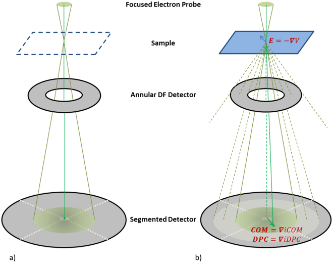
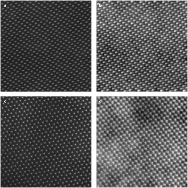
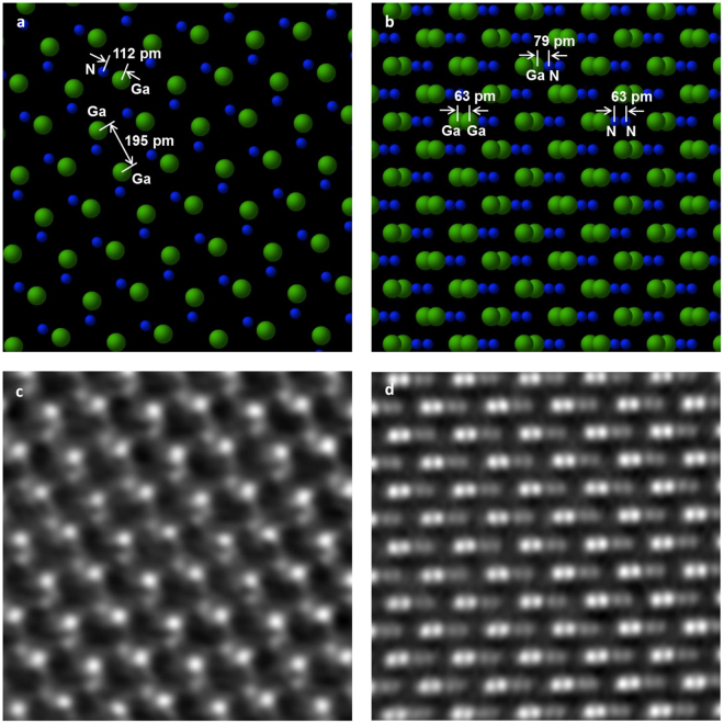
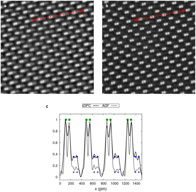
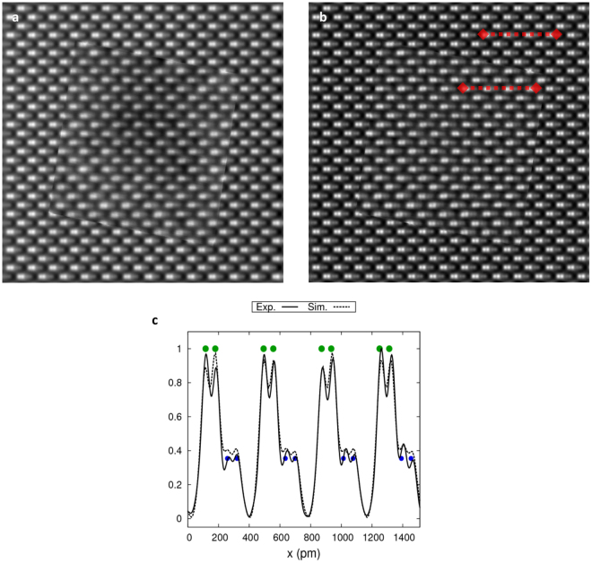
Using state of the art scanning transmission electron microscopy (STEM) it is nowadays possible to directly image single atomic columns at sub-Å resolution. In standard (high angle) annular dark field STEM ((HA)ADF-STEM), however, light elements are usually invisible when imaged together with heavier elements in one image. Here we demonstrate the capability of the recently introduced Integrated Differential Phase Contrast STEM (iDPC-STEM) technique to image both light and heavy atoms in a thin sample at sub-Å resolution. We use the technique to resolve both the Gallium and Nitrogen dumbbells in a GaN crystal in [[Formula: see text]] orientation, which each have a separation of only 63 pm. Reaching this ultimate resolution even for light elements is possible due to the fact that iDPC-STEM is a direct phase imaging technique that allows fine-tuning the microscope while imaging. Apart from this qualitative imaging result, we also demonstrate a quantitative match of ratios of the measured intensities with theoretical predictions based on simulations.
Conflict of interest statement
The authors declare no competing interests.
Figures
Similar articles
-
Optimizing experimental parameters of integrated differential phase contrast (iDPC) for atomic resolution imaging.Ultramicroscopy. 2023 Apr;246:113686. doi: 10.1016/j.ultramic.2023.113686. Epub 2023 Jan 18. Ultramicroscopy. 2023. PMID: 36682324
-
Phase contrast STEM for thin samples: Integrated differential phase contrast.Ultramicroscopy. 2016 Jan;160:265-280. doi: 10.1016/j.ultramic.2015.10.011. Epub 2015 Oct 19. Ultramicroscopy. 2016. PMID: 26590505
-
Imaging biological samples by integrated differential phase contrast (iDPC) STEM technique.J Struct Biol. 2022 Mar;214(1):107837. doi: 10.1016/j.jsb.2022.107837. Epub 2022 Jan 31. J Struct Biol. 2022. PMID: 35104612
-
Grain boundary atomic structures and light-element visualization in ceramics: combination of Cs-corrected scanning transmission electron microscopy and first-principles calculations.J Electron Microsc (Tokyo). 2011;60 Suppl 1:S173-88. doi: 10.1093/jmicro/dfr049. J Electron Microsc (Tokyo). 2011. PMID: 21844588 Review.
-
Coherent Diffraction Imaging in Transmission Electron Microscopy for Atomic Resolution Quantitative Studies of the Matter.Materials (Basel). 2018 Nov 19;11(11):2323. doi: 10.3390/ma11112323. Materials (Basel). 2018. PMID: 30463217 Free PMC article. Review.
Cited by
-
Structural Phase Transition and In-Situ Energy Storage Pathway in Nonpolar Materials: A Review.Materials (Basel). 2021 Dec 18;14(24):7854. doi: 10.3390/ma14247854. Materials (Basel). 2021. PMID: 34947446 Free PMC article. Review.
-
Unraveling the Atomistic Mechanisms Underlying Effective Reverse Osmosis Filtration by Graphene Oxide Membranes.Small Methods. 2025 Jan;9(1):e2400323. doi: 10.1002/smtd.202400323. Epub 2024 Jun 28. Small Methods. 2025. PMID: 38940224 Free PMC article.
-
Two-dimensional superconducting MoSi2N4(MoN)4n homologous compounds.Natl Sci Rev. 2022 Nov 28;10(4):nwac273. doi: 10.1093/nsr/nwac273. eCollection 2023 Apr. Natl Sci Rev. 2022. PMID: 39104911 Free PMC article.
-
Near-room temperature ferromagnetic insulating state in highly distorted LaCoO2.5 with CoO5 square pyramids.Nat Commun. 2021 Mar 25;12(1):1853. doi: 10.1038/s41467-021-22099-y. Nat Commun. 2021. PMID: 33767171 Free PMC article.
-
Manipulating the ordered oxygen complexes to achieve high strength and ductility in medium-entropy alloys.Nat Commun. 2023 Feb 13;14(1):806. doi: 10.1038/s41467-023-36319-0. Nat Commun. 2023. PMID: 36781880 Free PMC article.
References
-
- Haider M, et al. Electron microscopy image enhanced. Nature. 1998;392:768–769. doi: 10.1038/33823. - DOI
LinkOut - more resources
Full Text Sources
Other Literature Sources
Research Materials
