

Mesoscopic physical removal of material using sliding nano-diamond contacts
- PMID: 29445103
- PMCID: PMC5813091
- DOI: 10.1038/s41598-018-21171-w
Mesoscopic physical removal of material using sliding nano-diamond contacts
Abstract
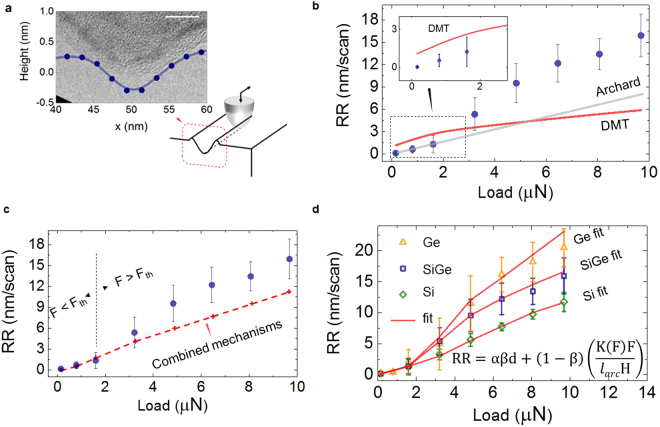
Wear mechanisms including fracture and plastic deformation at the nanoscale are central to understand sliding contacts. Recently, the combination of tip-induced material erosion with the sensing capability of secondary imaging modes of AFM, has enabled a slice-and-view tomographic technique named AFM tomography or Scalpel SPM. However, the elusive laws governing nanoscale wear and the large quantity of atoms involved in the tip-sample contact, require a dedicated mesoscale description to understand and model the tip-induced material removal. Here, we study nanosized sliding contacts made of diamond in the regime whereby thousands of nm3 are removed. We explore the fundamentals of high-pressure tip-induced material removal for various materials. Changes in the load force are systematically combined with AFM and SEM to increase the understanding and the process controllability. The nonlinear variation of the removal rate with the load force is interpreted as a combination of two contact regimes each dominating in a particular force range. By using the gradual transition between the two regimes, (1) the experimental rate of material eroded on each tip passage is modeled, (2) a controllable removal rate below 5 nm/scan for all the materials is demonstrated, thus opening to future development of 3D tomographic AFM.
Conflict of interest statement
The authors declare no competing interests.
Figures
Similar articles
-
Mechanics of interaction and atomic-scale wear of amplitude modulation atomic force microscopy probes.ACS Nano. 2013 Apr 23;7(4):3221-35. doi: 10.1021/nn305901n. Epub 2013 Mar 29. ACS Nano. 2013. PMID: 23506316
-
Tribochemical Wear of Diamond-Like Carbon-Coated Atomic Force Microscope Tips.ACS Appl Mater Interfaces. 2017 Oct 11;9(40):35341-35348. doi: 10.1021/acsami.7b08026. Epub 2017 Sep 29. ACS Appl Mater Interfaces. 2017. PMID: 28960949
-
Atomic-scale wear of amorphous hydrogenated carbon during intermittent contact: a combined study using experiment, simulation, and theory.ACS Nano. 2014 Jul 22;8(7):7027-40. doi: 10.1021/nn501896e. Epub 2014 Jun 25. ACS Nano. 2014. PMID: 24922087
-
Mechanisms of friction reduction of nanoscale sliding contacts achieved through ultrasonic excitation.Nanotechnology. 2019 Feb 15;30(7):075502. doi: 10.1088/1361-6528/aaf3cd. Epub 2018 Nov 26. Nanotechnology. 2019. PMID: 30523838
-
Method for characterizing nanoscale wear of atomic force microscope tips.ACS Nano. 2010 Jul 27;4(7):3763-72. doi: 10.1021/nn100246g. ACS Nano. 2010. PMID: 20575565
Cited by
-
Understanding Current Instabilities in Conductive Atomic Force Microscopy.Materials (Basel). 2019 Feb 1;12(3):459. doi: 10.3390/ma12030459. Materials (Basel). 2019. PMID: 30717254 Free PMC article.
-
Asperity level characterization of abrasive wear using atomic force microscopy.Proc Math Phys Eng Sci. 2021 Jun;477(2250):20210103. doi: 10.1098/rspa.2021.0103. Epub 2021 Jun 9. Proc Math Phys Eng Sci. 2021. PMID: 35153566 Free PMC article.
-
Nanoscale cutting using self-excited microcantilever.Sci Rep. 2022 Jan 12;12(1):618. doi: 10.1038/s41598-021-04085-y. Sci Rep. 2022. PMID: 35022414 Free PMC article.
References
-
- Celano, U. Metrology and Physical Mechanisms in New Generation Ionic Devices. (Springer International Publishing, 10.1007/978-3-319-39531-9 (2016).
-
- Luria J, et al. Charge transport in CdTe solar cells revealed by conductive tomographic atomic force microscopy. Nat. Energy. 2016;1:16150. doi: 10.1038/nenergy.2016.150. - DOI
-
- Conductive Atomic Force Microscopy: Applications in Nanomaterials. (Wiley-VCH Verlag GmbH & Co. KGaA 10.1002/9783527699773 (2017).
-
- Buckwell M, et al. Conductive AFM Topography of Intrinsic Conductivity Variations in Silica Based Dielectrics for Memory Applications. ECS Trans. 2016;75:3–9. doi: 10.1149/07505.0003ecst. - DOI
Publication types
LinkOut - more resources
Full Text Sources
Other Literature Sources
Miscellaneous
