

Quantum and electrochemical interplays in hydrogenated graphene
- PMID: 29476098
- PMCID: PMC5824792
- DOI: 10.1038/s41467-018-03026-0
Quantum and electrochemical interplays in hydrogenated graphene
Abstract
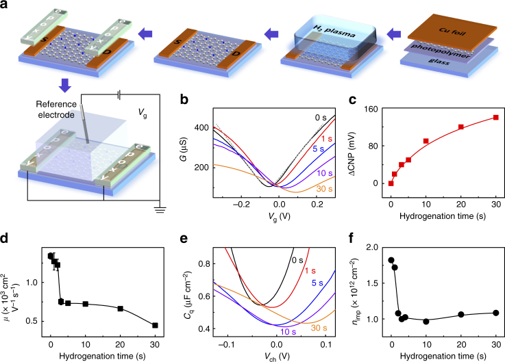
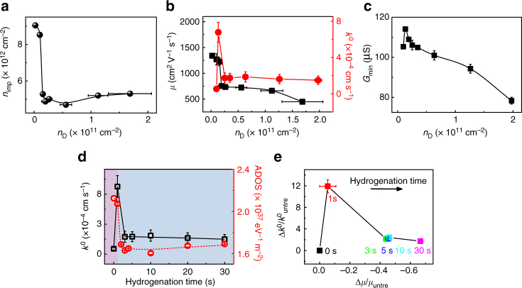
The design of electrochemically gated graphene field-effect transistors for detecting charged species in real time, greatly depends on our ability to understand and maintain a low level of electrochemical current. Here, we exploit the interplay between the electrical in-plane transport and the electrochemical activity of graphene. We found that the addition of one H-sp3 defect per hundred thousand carbon atoms reduces the electron transfer rate of the graphene basal plane by more than five times while preserving its excellent carrier mobility. Remarkably, the quantum capacitance provides insight into the changes of the electronic structure of graphene upon hydrogenation, which predicts well the suppression of the electrochemical activity based on the non-adiabatic theory of electron transfer. Thus, our work unravels the interplay between the quantum transport and electrochemical kinetics of graphene and suggests hydrogenated graphene as a potent material for sensing applications with performances going beyond previously reported graphene transistor-based sensors.
Conflict of interest statement
The authors declare no competing financial interests.
Figures


Similar articles
-
Graphene field-effect transistors: electrochemical gating, interfacial capacitance, and biosensing applications.Chem Asian J. 2010 Oct 4;5(10):2144-53. doi: 10.1002/asia.201000252. Chem Asian J. 2010. PMID: 20715049 Review.
-
Electrochemical properties of CVD grown pristine graphene: monolayer- vs. quasi-graphene.Nanoscale. 2014;6(3):1607-21. doi: 10.1039/c3nr05643k. Nanoscale. 2014. PMID: 24337073
-
Controlled hydrogenation of graphene sheets and nanoribbons.ACS Nano. 2011 Feb 22;5(2):888-96. doi: 10.1021/nn102034y. Epub 2011 Jan 28. ACS Nano. 2011. PMID: 21275382
-
Highly hydrogenated graphene through microwave exfoliation of graphite oxide in hydrogen plasma: towards electrochemical applications.Chemistry. 2013 Nov 11;19(46):15583-92. doi: 10.1002/chem.201303164. Epub 2013 Oct 7. Chemistry. 2013. PMID: 24123303
-
Electrochemical sensors and biosensors based on less aggregated graphene.Biosens Bioelectron. 2017 Mar 15;89(Pt 1):167-186. doi: 10.1016/j.bios.2016.05.002. Epub 2016 May 3. Biosens Bioelectron. 2017. PMID: 27161575 Review.
Cited by
-
Graphene-enhanced Raman scattering on single layer and bilayers of pristine and hydrogenated graphene.Sci Rep. 2020 Mar 11;10(1):4516. doi: 10.1038/s41598-020-60857-y. Sci Rep. 2020. PMID: 32161329 Free PMC article.
-
A versatile route to edge-specific modifications to pristine graphene by electrophilic aromatic substitution.J Mater Sci. 2020;55(24):10284-10302. doi: 10.1007/s10853-020-04662-y. Epub 2020 May 9. J Mater Sci. 2020. PMID: 32536720 Free PMC article.
-
Carbon-Based Quantum Dots for Supercapacitors: Recent Advances and Future Challenges.Nanomaterials (Basel). 2021 Jan 3;11(1):91. doi: 10.3390/nano11010091. Nanomaterials (Basel). 2021. PMID: 33401630 Free PMC article. Review.
-
Versatile Confocal Raman Imaging Microscope Built from Off-the-Shelf Opto-Mechanical Components.Sensors (Basel). 2022 Dec 19;22(24):10013. doi: 10.3390/s222410013. Sensors (Basel). 2022. PMID: 36560382 Free PMC article.
-
Quantitative Principles for Precise Engineering of Sensitivity in Graphene Electrochemical Sensors.Adv Mater. 2019 Feb;31(6):e1805752. doi: 10.1002/adma.201805752. Epub 2018 Dec 13. Adv Mater. 2019. PMID: 30548684 Free PMC article.
References
Publication types
Grants and funding
LinkOut - more resources
Full Text Sources
Other Literature Sources
Molecular Biology Databases
