. 2018 Mar 2;4(3):eaao5031.
doi: 10.1126/sciadv.aao5031. eCollection 2018 Mar.

Oxide-mediated recovery of field-effect mobility in plasma-treated MoS2

Affiliations

Oxide-mediated recovery of field-effect mobility in plasma-treated MoS2

Jakub Jadwiszczak et al. Sci Adv. .

Abstract

Precise tunability of electronic properties of two-dimensional (2D) nanomaterials is a key goal of current research in this field of materials science. Chemical modification of layered transition metal dichalcogenides leads to the creation of heterostructures of low-dimensional variants of these materials. In particular, the effect of oxygen-containing plasma treatment on molybdenum disulfide (MoS2) has long been thought to be detrimental to the electrical performance of the material. We show that the mobility and conductivity of MoS2 can be precisely controlled and improved by systematic exposure to oxygen/argon plasma and characterize the material using advanced spectroscopy and microscopy. Through complementary theoretical modeling, which confirms conductivity enhancement, we infer the role of a transient 2D substoichiometric phase of molybdenum trioxide (2D-MoO x ) in modulating the electronic behavior of the material. Deduction of the beneficial role of MoO x will serve to open the field to new approaches with regard to the tunability of 2D semiconductors by their low-dimensional oxides in nano-modified heterostructures.


Figures

Fig. 1
Fig. 1. Characterization of the 4L device.
Note that (A), (B), and (E) share the same color legend and that all measurements were performed at room temperature. (A) I-V curve evolution over exposure time. All curves are measured at zero gate bias. We note the increased current density observed after 6 s (red). (B) Gate sweeps of the same device over exposure time. The curves after 6, 8, and 10 s show a largely linear response in the semi-log plot at low gate biases and do not reach threshold over standard sweep range. Subsequent treatment until 12 s drastically shifts VTH to positive gate biases and lowers the current by several orders of magnitude. (C) Threshold voltage for the same device shows a sudden drop at 6 s followed by a steady increase to extremely positive gate biases over treatment time. (D) Subthreshold swing variation with exposure time shows a diminished response to the gate field starting at 6 s. The area marked in green in (C) and (D) indicates the electrical recovery region. (E) Extraction of field-effect mobility for the same 4L device across the whole gate bias range (graph begins from −40 V for clarity). The peak mobility reached in the curves is seen to degrade over time. The green region marks the area of the gate sweep where the 6-s exposure attains highest relative mobility values (red curve). (F) Mobility change over plasma treatment time extracted at gate biases between −60 and 60 V. The color legend explicitly maps the curves onto different regions of the gate sweep. The increase at 6 s is visualized in the form of rising recovery peaks in the body of the plot, which correspond to 6-s mobilities evaluated in the green area marked in (E).
Fig. 2
Fig. 2. Surface morphology of plasma-treated MoS2.
(A to C) Phase maps of the same region of a 4L flake, showing notable material contrast on the surface as oxides are formed over time. Scale bars, 200 nm. (D) Chart of edge heights extracted along line profiles after each exposure time (see all the raw height maps in fig. S11). The region in green is the edge height peak, which correlates with the electrical recovery time at 6 s. (E) Root mean square (RMS) surface roughness profiles extracted over time from height maps of the 4L and 5L regions of the flake. (F) AFM map of bottom edge of this flake after 28 s of plasma etching. Visible voids are seen along the bottom of the sample (G) scanning electron microscopy (SEM) image of the corner of the same flake, exhibiting dark contrast pits on the edge, corresponding to oxidized MoS2 regions.
Fig. 3
Fig. 3. Spectroscopic signatures of oxidized MoS2.
(A) Raman spectrum of 4L MoS2 over plasma treatment time shown in the semi-log plot. The inset tracks the time evolution of the separation between the E2g1 and A1g peaks. (B) PL spectrum of 4L MoS2 as it changes over plasma exposure time, showing significant A exciton enhancement at 6 s of treatment. au, arbitrary units. (C) Left: Time evolution of EDX spectrum normalized to the sulfur-Kα line taken from a suspended 4L flake. Right: Ratio of O/S elemental signal intensity tracked over exposure time. The green line is a linear fit to the data. (D) Areal EDX mapping of sulfur (red) and oxygen (green) content in the same 4L sample at 0, 6, and 10 s of plasma treatment. The associated histograms visualize the intensity distribution of the green oxygen pixels in the maps. Scale bar, 500 nm. (E) XPS spectra of the Mo 3d region showing increased MoO3 content overtime. (F) S 2p region of the XPS spectrum.
Fig. 4
Fig. 4. Evidence of oxide-mediated etching on the nanoscale.
(A) Typical AC-STEM micrograph showing nanoscale voids forming in bilayer MoS2 after 6 s of plasma exposure. The region marked in magenta shows an etched pit with part of the top layer missing. The area marked in orange shows a perforation where no material remains. (B) Scatterplot and histograms visualizing the distribution of the lateral dimensions of etched voids on this flake after 6 s of plasma exposure. The scatter data are color-mapped from cool to warm with increasing void width.
Fig. 5
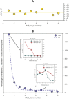
Fig. 5. Effect of layer number on mobility recovery.
(A) Change in gate threshold voltage between recovery time and pristine MoS2 tracked as a function of layer number. Devices of all thicknesses show a major VTH shift to negative gate bias at the time of mobility recovery. The mean shift value of −19 V is marked by the horizontal yellow line. (B) Percentage increase in subthreshold swing between untreated and recovered stages for samples of all tested thicknesses. Ssub increases for all samples at the recovery stage and the effect scales with MoS2 layer number. Insets track the mobility evolution over exposure time for the 1L and 7L samples in the linear (green) and saturation (red) regimes. The mobility recovery happens for samples thicker than two layers.
Fig. 6
Fig. 6. Resistive network simulation of oxidized MoS2.
Simulated sheet conductance of MoS2 during the progressive conversion from MoS2 to 2D-MoOx to MoO3. Exposure time, which is expressed in arbitrary units, charts the progress of the plasma-induced chemical oxidation as the simulation is iterated. One site undergoes transformation to the next phase during each iteration. Sites are not destroyed in this simulation, and the plasma-etching process finishes when all sites reach the insulating MoO3 phase. The distribution of phases in the conductive network at four different iteration stages is shown throughout (i) to (iv), where the subsequent phases are color-mapped to the scale shown on the right. The lattice visualized in (ii) corresponds to the state of the network at the recovery time. The concentration of 2D-MoOx at that stage is ≈15%.

References

    1. Radisavljevic B., Radenovic A., Brivio J., Giacometti V., Kis A., Single-layer MoS2 transistors. Nat. Nanotechnol. 6, 147–150 (2011). - PubMed
    1. Radisavljevic B., Kis A., Mobility engineering and a metal–insulator transition in monolayer MoS2. Nat. Mater. 12, 815–820 (2013). - PubMed
    1. Jariwala D., Sangwan V. K., Lauhon L. J., Marks T. J., Hersam M. C., Emerging device applications for semiconducting two-dimensional transition metal dichalcogenides. ACS Nano 8, 1102–1120 (2014). - PubMed
    1. Lembke D., Bertolazzi S., Kis A., Single-layer MoS2 electronics. Acc. Chem. Res. 48, 100–110 (2015). - PubMed
    1. Sangwan V. K., Jariwala D., Kim I. S., Chen K.-S., Marks T. J., Lauhon L. J., Hersam M. C., Gate-tunable memristive phenomena mediated by grain boundaries in single-layer MoS2. Nat. Nanotechnol. 10, 403–406 (2015). - PubMed

Publication types

LinkOut - more resources