Review
. 2018 Mar 23;8(4):188.
doi: 10.3390/nano8040188.

1D Piezoelectric Material Based Nanogenerators: Methods, Materials and Property Optimization

Affiliations
Review

1D Piezoelectric Material Based Nanogenerators: Methods, Materials and Property Optimization

Xing Li et al. Nanomaterials (Basel). .

Abstract

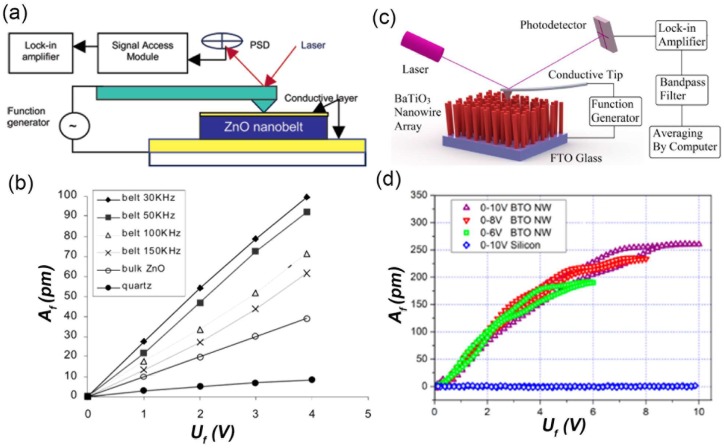
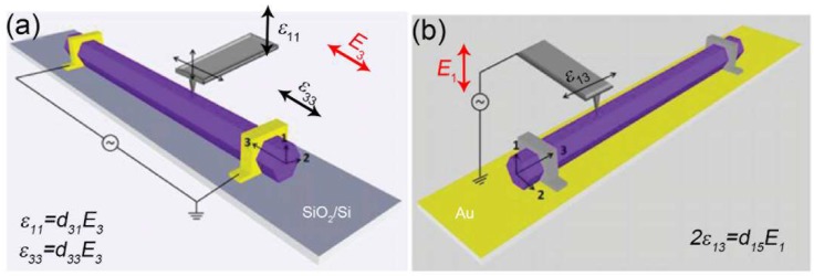
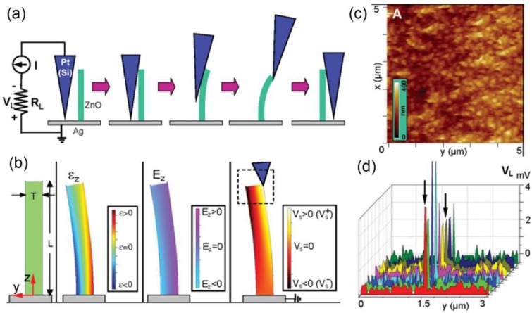
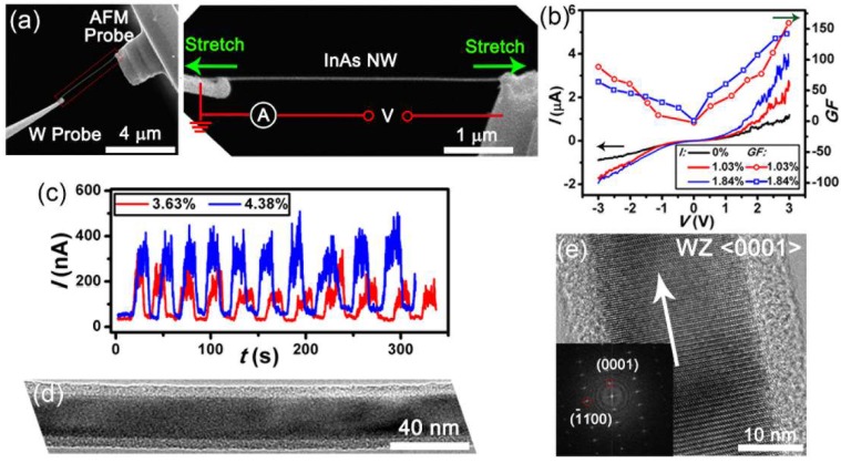
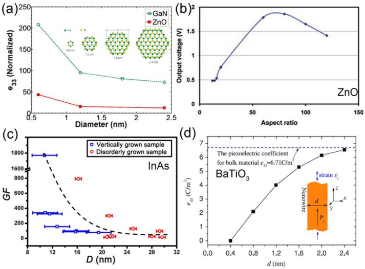
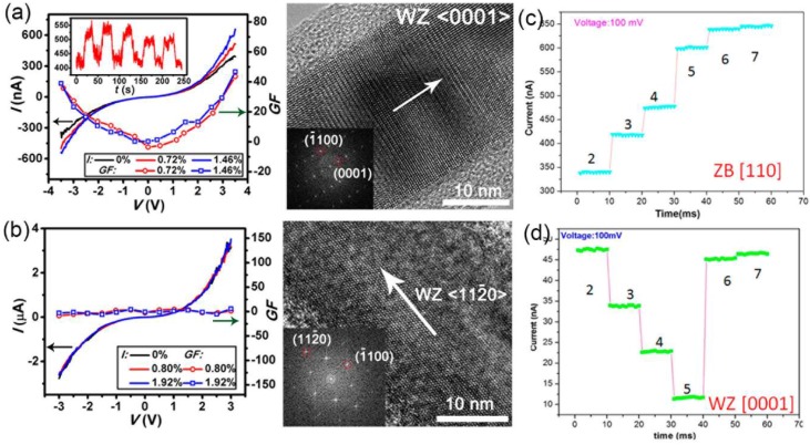
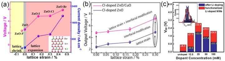
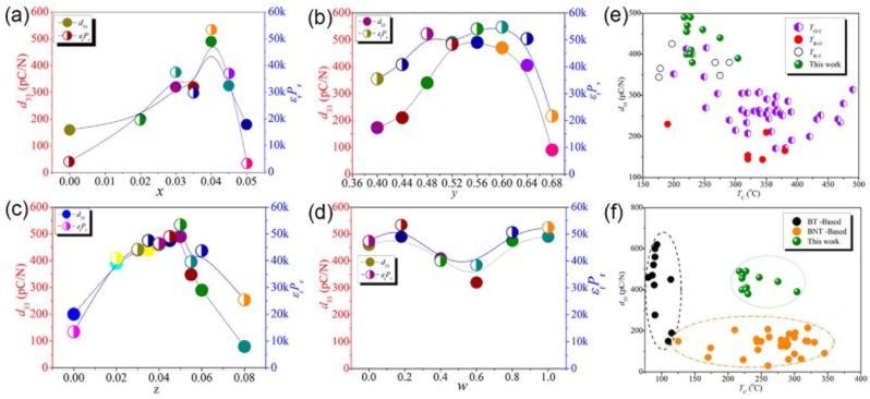
Due to the enhanced piezoelectric properties, excellent mechanical properties and tunable electric properties, one-dimensional (1D) piezoelectric materials have shown their promising applications in nanogenerators (NG), sensors, actuators, electronic devices etc. To present a clear view about 1D piezoelectric materials, this review mainly focuses on the characterization and optimization of the piezoelectric properties of 1D nanomaterials, including semiconducting nanowires (NWs) with wurtzite and/or zinc blend phases, perovskite NWs and 1D polymers. Specifically, the piezoelectric coefficients, performance of single NW-based NG and structure-dependent electromechanical properties of 1D nanostructured materials can be respectively investigated through piezoresponse force microscopy, atomic force microscopy and the in-situ scanning/transmission electron microcopy. Along with the introduction of the mechanism and piezoelectric properties of 1D semiconductor, perovskite materials and polymers, their performance improvement strategies are summarized from the view of microstructures, including size-effect, crystal structure, orientation and defects. Finally, the extension of 1D piezoelectric materials in field effect transistors and optoelectronic devices are simply introduced.

Keywords: 1D piezoelectric materials; characterization methods; defects; piezoelectric property optimization; size effect; structure and orientation dependence.


Conflict of interest statement

The authors declare no conflict of interest.

Figures

Figure 1
Figure 1
The piezoelectric coefficient measurement with the piezoresponse force microscopy (PFM) method. (a) The schematic diagram of experimental setup of the PFM method in measuring d33 along the radial direction of the lateral dispersed one dimensional (1D) nanostructures; (b) The Af-Uf curve obtained with the PFM method, the piezoelectric coefficient can be obtained from the slope of the linear curve. Reproduced with permission from [36]. American Chemical Society, 2004; (c) The schematic diagram of the experimental setup of the refined PFM method in measuring d33 along the axial direction of the vertically grown nanowire (NW) array; (d) The Af-Uf curve of a BaTiO3 NW with refined PFM method. Reproduced with permission from [41]. American Chemical Society, 2013.
Figure 2
Figure 2
The schematic representations of measurement configurations for probing the piezoelectric coefficients of (a) d33, d31 and (b) d15 of a single c-axis GaN NW. Reproduced with permission from [23]. American Chemical Society, 2011.
Figure 3
Figure 3
Piezoelectric nanogenerator (NG) investigated with the atomic force microscopy (AFM) lateral bending method. (a) Experimental setup and procedures for generating electricity by deforming a vertically grown ZnO NW with a conductive AFM tip; (b) Simulation results of the longitudinal strain, corresponding piezoelectric induced electric field and potential for a bended ZnO NW; (c) The topography image of the measured ZnO NW array; (d) A series of line profiles of the voltage output signal when the AFM tip scanned across a vertical NW at a time interval of 1 min. Reproduced with permission from [5]. The American Association for the Advancement of Science, 2006.
Figure 4
Figure 4
In-situ scanning electron microscopy (SEM) tensile test in measuring the piezoelectric and piezoresistive effects of InAs NWs. (a) SEM image showing the experimental setup for the electromechanical measurement of InAs NWs; (b) The measured current-voltage (I-V) and gauge factor-voltage (GF-V) curves and (c) the electrical current responses of InAs NWs; (d) The low-magnification and (e) high-resolution transmission electron microscope (TEM) images of the NW measured in (b). Reproduced with permission from [24]. John Wiley and Sons, 2015.
Figure 5
Figure 5
(a) The piezoelectric charge detection from an individual BaTiO3 NW with the tensile loading platform. Reproduced with permission from [54]. American Chemical Society, 2007; (b) SEM images showing the manipulation process for an individual InAs NW with a dual beam system; (c) TEM images showing the in-situ TEM deformation process of an InAs NW and corresponding I-V curves to each deformation state. Reproduced with permission from [56]. American Chemical Society, 2016.
Figure 6
Figure 6
(a) Atomic model of wurtzite (WZ) ZnO and the compressive strain induced dipole moment; (b) Vertically aligned ZnO NW arrays and simulated piezoelectric potential along a ZnO NW under axial strain along the c-axis direction. Reproduced with permission from [59]. John Wiley and Sons, 2012. 3D electric signal images of (c) undoped AlN (10−11–10−13 Ω−1·cm−1); (d) Al0.35Ga0.65N (~0.5 Ω−1·cm−1); (e) GaN (~6–12 Ω−1·cm−1); (f) InN (~200–300 Ω−1·cm−1). Reproduced with permission from [46]. John Wiley and Sons, 2010.
Figure 7
Figure 7
Atomic model of (a) cubic perovskite structure and (b) rhombohedral LiNbO3 structure; (c) Schematic diagram of the NaNbO3 based flexible NG and (d) its power generation mechanism. Reproduced with permission from [71]. American Chemical Society, 2011.
Figure 8
Figure 8
Schematic depiction of (a) α-phase (left) and β-phase (right) of the crystalline chain conformation of PVDF. The arrows indicate projections of the -CF2 dipole direction on planes defined by the carbon backbone. Reproduced with permission from [76]. the American Association for the Advancement of Science, 1983; (b) Scheme diagram of the molecular orientation of the polymeric chain templated in the mesoporous host. Both the a- and c-axes are in-plane with the alumina surface and the b-axis, as well as the polarization axis P, are aligned with the long axis of the NWs. Reproduced with permission from [80]. American Chemical Society, 2012.
Figure 9
Figure 9
(a) The piezoelectric coefficient of GaN and ZnO NWs as a function of their diameter. Reproduced with permission from [94]. American Chemical Society, 2011; (b) The output electrical potential vs. aspect ratio of ZnO NWs controlled at constant diameter of 50 nm and changing the NW length from 600 to 6000 nm. Reproduced with permission from [95]. John Wiley and Sons, 2011; (c) The GF of InAs NWs with different diameters. Reproduced with permission from [24]. John Wiley and Sons, 2015; (d) The size-dependent piezoelectric coefficient of BaTiO3 NW. Reproduced with permission from [96]. IOP Publishing Ltd., 2010.
Figure 10
Figure 10
I-V, GF-V curves and corresponding high resolution TEM images of (a) <0001> orientated WZ InAs NW with stacking faults and (b) single-crystalline <112¯0> oriented WZ InAs NW at different axial tensile strains. Reproduced with permission from [24]. John Wiley and Sons, 2015. The variation of the electrical current with increasing deformation of (c) a <110> orientated zinc blend (ZB) InAs NW and (d) a <0001> orientated WZ InAs NW. Reproduced with permission from [56]. American Chemical Society, 2016.
Figure 11
Figure 11
(a) The dependence of the output performance of ZnO piezoelectric NG on the lattice strain induced by different halogen dopant. Reproduced with permission from [108]. American Chemical Society, 2015; (b) Output performance of ZnO NW film NG as a function of the doping concentration of Cl. Reproduced with permission from [114]. American Chemical Society, 2016; (c) Histogram of piezoelectric output voltages for undoped and Li-doped ZnO NW samples and the influence of surface functionalization. Reproduced with permission from [113]. The Royal Society of Chemistry, 2013.
Figure 12
Figure 12
The change of d33 with chemical composition of (1 − x)(K1−yNay)(Nb1−zSbz)O3−xBi0.5(Na1−wKw)0.5ZrO3 at (a) y = 0.52, z = 0.05, w = 0.18; (b) x = 0.04, z = 0.05, w = 0.18; (c) x = 0.04, y = 0.52, w = 0.18; (d) x = 0.04, y = 0.52, z = 0.05. d33 as a function of TC for (e) KNN-based piezoceramics and the (1 − x)(K1−yNay)(Nb1−zSbz)O3−xBi0.5(Na1−wKw)0.5ZrO3 ceramics and (f) Bi0.5Na0.5TiO3 (BNT)- and BaTiO3 (BT)-based piezoceramics and the (1 − x)(K1−yNay)(Nb1−zSbz)O3−xBi0.5(Na1−wKw)0.5ZrO3 ceramics. Reproduced with permission from [119]. American Chemical Society, 2014.

Similar articles

Cited by

References

    1. Liu Y., Wang S., Liu H., Peng L.M. Carbon nanotube-based three-dimensional monolithic optoelectronic integrated system. Nat. Commun. 2017;8:15649. doi: 10.1038/ncomms15649. - DOI - PMC - PubMed
    1. Wu G., Wei X., Gao S., Chen Q., Peng L. Tunable graphene micro-emitters with fast temporal response and controllable electron emission. Nat. Commun. 2016;7:11513. doi: 10.1038/ncomms11513. - DOI - PMC - PubMed
    1. Ding L., Zhang Z., Liang S., Pei T., Wang S., Li Y., Zhou W., Liu J., Peng L.M. CMOS-based carbon nanotube pass-transistor logic integrated circuits. Nat. Commun. 2012;3:677. doi: 10.1038/ncomms1682. - DOI - PMC - PubMed
    1. Shang Y., Hua C., Xu W., Hu X., Wang Y., Zhou Y., Zhang Y., Li X., Cao A. Meter-long spiral carbon nanotube fibers show ultrauniformity and flexibility. Nano Lett. 2016;16:1768–1775. doi: 10.1021/acs.nanolett.5b04773. - DOI - PubMed
    1. Wang Z.L., Song J. Piezoelectric nanogenerators based on zinc oxide nanowire arrays. Science. 2006;312:242–246. doi: 10.1126/science.1124005. - DOI - PubMed

LinkOut - more resources